Spontaneous emission display, spontaneous emission display manufacturing method, transparent conductive film, electroluminescence device, solar cell transparent electrode, and electronic paper transparent electrode

a technology of spontaneous emission and manufacturing method, which is applied in the direction of sustainable manufacturing/processing, identification means, instruments, etc., can solve the problems of high cost, high temperature treatment, and disadvantages of transparent conductive layers in low light transmittance, and achieve low cost, low surface resistance, and low cost

Active Publication Date: 2009-12-03
FUJIFILM CORP
View PDF4 Cites 31 Cited by
  • Summary
  • Abstract
  • Description
  • Claims
  • Application Information

AI Technical Summary

Benefits of technology

[0079]The ITO layer does not have a sufficiently low surface resistance. In contrast, since the conductive layer and the thin-wire structure portion are used in combination, the transparent conductive film of the present invention can have a low surface resistance and can be formed at low cost, and thereby can be utilized in an inorganic EL, a solar cell, etc.
[0080]Even in the case of using the transparent conductive film in a large-size EL device, the luminance of the device is hardly lowered by the transparent conductive film since the thin-wire structure portion has a surface resistance lower tha...

Problems solved by technology

Thus, the transparent conductive layer is disadvantageous in low light transmittance, high cost, and that a high temperature treatment is needed in the formation process.
The methods described in Patent Documents 1 and 2, etc., which include vapor-depositing or sputtering a transparent electrode layer of a conductive metal, such as an ITO (Indium Tin Oxide) layer, to increase conductivity, are poor in productivity, and need improvement on this point.
Furthermore, in the method using the busline, the number of processes is increased, thereby resulting in high cost.
However, there are fears of depletion of the ITO, and thus an alternative material is demanded.
In addition, great loss is disadvantageously caused in the vapor deposition process.
However, the method is uns...

Method used


Image

  • Spontaneous emission display, spontaneous emission display manufacturing method, transparent conductive film, electroluminescence device, solar cell transparent electrode, and electronic paper transparent electrode
  • Spontaneous emission display, spontaneous emission display manufacturing method, transparent conductive film, electroluminescence device, solar cell transparent electrode, and electronic paper transparent electrode
  • Spontaneous emission display, spontaneous emission display manufacturing method, transparent conductive film, electroluminescence device, solar cell transparent electrode, and electronic paper transparent electrode

Examples


first example

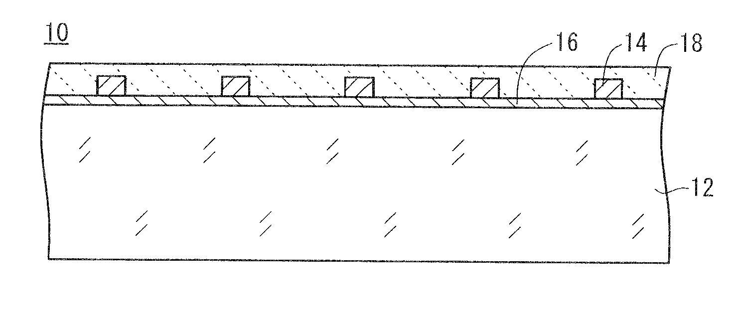
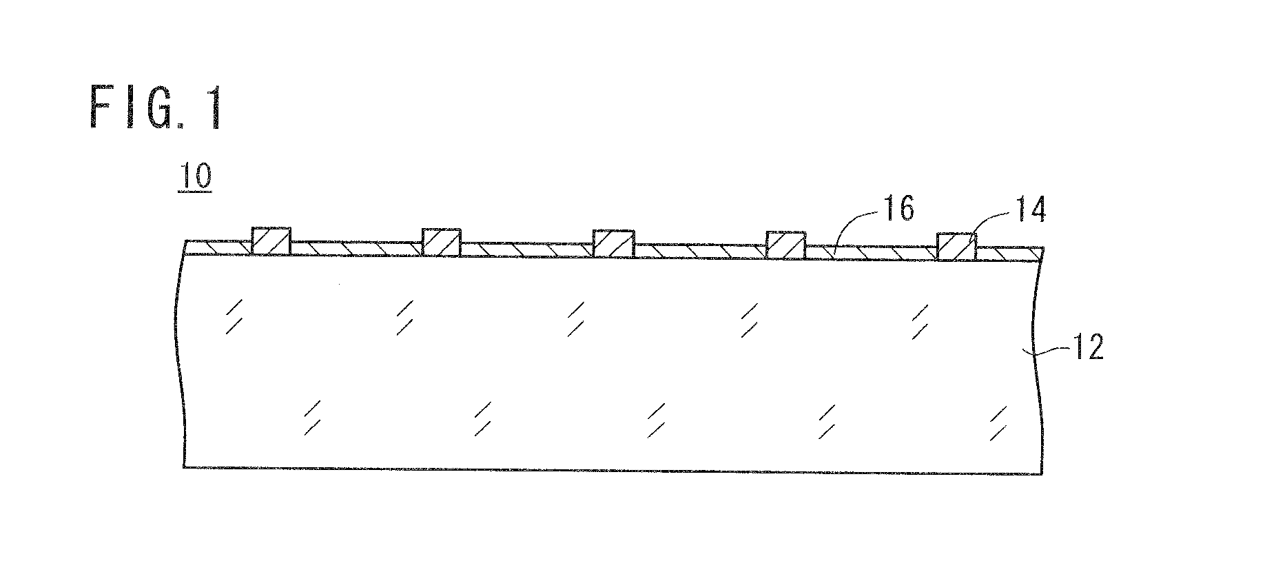
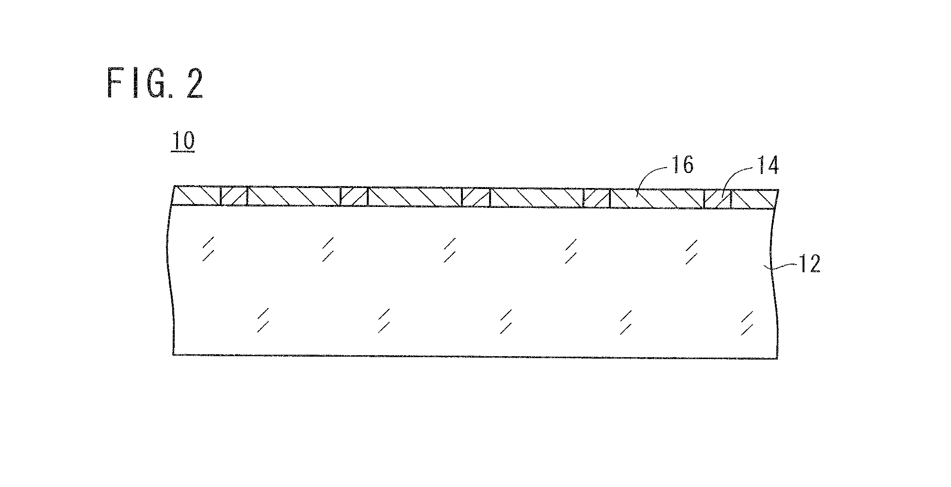
[0316]First Example is described below. The properties (surface resistance, film strength, etc.) of the thin-wire structure portion 14 formed on the support 12 were evaluated in First Example.

Examples 1 to 14 and Comparative Examples 1 to 7

[0317]

(Preparation of Emulsion A)Liquid 1Water750mlGelatin (phthalated gelatin)20gSodium chloride3g1,3-Dimethylimidazolidine-2-thione20mgSodium benzenethiosulfonate10mgCitric acid0.7gLiquid 2Water300mlSilver nitrate150gLiquid 3Water300mlSodium chloride38gPotassium bromide32gPotassium hexachloroiridate (III)5ml(0.005% KCl, 20% aqueous solution)Ammonium hexachlororhodate7ml(0.001% NaCl, 20% aqueous solution)

[0318]The potassium hexachloroiridate (III) (0.005% KCl, 20% aqueous solution) and the ammonium hexachlororhodate (0.001% NaCl, 20% aqueous solution) in Liquid 3 were prepared by dissolving a complex powder in a 20% aqueous solution of KCl and a 20% aqueous solution of NaCl, respectively, and by heating the resultant solutions at 40° C. for 120 m...

second example

[0366]Among the samples of Examples 1 to 14 shown in Table 1, the sample of Example 14, which was produced by carrying out the calender treatment after the development and also after the fixation, had the lowest surface resistivity of 0.08 (Ω / sq).

[0367]Thus, the relation between line pressure and surface resistivity in the calender treatment after development and the calender treatment after fixation was examined. The results are shown in FIG. 10.

[0368]Sample B-a-2 (see Example 3) was used in this example. The sample was exposed and developed in the same manner as above, and then washed with pure water for 1 minute, and dried at 40° C. The dried sample was subjected to a calender treatment after development, and subjected to a fixation treatment using a fixer N3X-R for CN16X (trade name, available from FUJIFILM Corporation). Then, the sample was washed with pure water for 2 minutes, dried, and subjected to a calender treatment after fixation.

[0369]Two calender roll units were used i...

third example

[0372]Third Example is described below. The properties (transmittance, volume resistance, surface resistance, flexibility, etc.) of the transparent conductive film 10 were evaluated in Third Example.

1. Production of Support 12 Having Thin-Wire Structure Portion 14

(Preparation of Emulsion)

[0373]An emulsion used in Third Example is the same as Emulsion A of First Example, and duplicate explanations therefor are omitted.

(Production of Coating Sample)

[0374]A coating sample used in Third Example is the same as Coating sample A using Emulsion A described in First Example, and duplicate explanations therefor are omitted.

[0375]In the obtained coating sample, the emulsion layer had an Ag / binder volume ratio of 1 / 0.7. Thus, the emulsion layer satisfies the Ag / binder ratio condition of 1 / 4 or more, which is preferably used in the present invention.

(Exposure and Development Treatments)

[0376]Then, the dried coating layer was exposed to a parallel light from a light source of a high-pressure merc...


PUM


Abstract

A spontaneous emission display includes a support, a first electrode section provided on the support and having a fine wire structure portion made of a conductive metal and a translucent conductive film, and a display section formed on the first electrode section and having a light-emitting layer. The volume resistance of the fine wire structure portion of the first electrode is 10−4 Ω·cm or less and/or the surface resistance thereof is 100 Ω/sq or less. The volume resistance of the conductive film is 0.05 Ω·cm or more and/or the surface resistance thereof is 100 Ω/sq or more. When the surface resistance of the first electrode section before a bending test is denoted by R1 and that after the bending test is denoted by R2, R2/R1<18 is satisfied.

Description

TECHNICAL FIELD[0001]The present invention relates to a self-luminous display device having an electrode region with high light transmittance, low surface resistivity, and excellent flexibility, a method for producing the display device, a transparent conductive film with high light transmittance, low surface resistivity, and excellent flexibility, and an electroluminescence device, a solar cell transparent electrode, and an electronic paper transparent electrode containing the transparent conductive film. The self-luminous display device may be a light-emitting device for lighting purpose.BACKGROUND ART[0002]In recent years, in liquid crystal displays, organic and inorganic electroluminescence devices, electronic papers, etc., a film or a glass substrate having a transparent conductive layer has been used as an electrode on the light-emitting side (see, for example, Patent Documents 1 to 4).[0003]The transparent conductive layer is generally composed of an indium tin oxide, a zinc ...

Claims


Application Information

Patent Timeline
IPC IPC(8): H01J1/62H05K1/09G03F1/00G02F1/15G02F1/167G09F9/30H01L27/32H01L31/04H01L51/50H05B33/10H05B33/14H05B33/26H05B33/28
CPCH01L27/32H01L51/0021H01L51/0064H01L51/5212H01L51/56H01L2251/5338H01L51/5206Y02E10/549Y02P70/50H10K71/60H10K85/652H10K50/814H10K2102/311H10K59/80516H10K59/00H10K71/00
Inventor TOKUNAGA, TSUKASAKUSUOKA, MAKOTOKURIKI, TADASHIICHIKI, AKIRA
Owner FUJIFILM CORP
Why Eureka
Try Eureka