Process for producing single-crystal substrate with off angle

a technology of single crystal substrate and off-angle, which is applied in the direction of crystal growth process, polycrystalline material growth, after-treatment details, etc., can solve the problems of diamond's excellent electrical properties not being fully displayed, electrical properties deteriorating, and diamond's electrical properties being deteriorated, etc., to achieve simple and short production period, increase the number of off-substrates, and high controllability

Inactive Publication Date: 2009-12-17
NAT INST OF ADVANCED IND SCI & TECH
View PDF7 Cites 16 Cited by
  • Summary
  • Abstract
  • Description
  • Claims
  • Application Information

AI Technical Summary

Benefits of technology

[0020]In accordance with the process of the invention, off-substrates, which have been conventionally produced by polishing, can be produced simply and in a short period of time, with extremely high controllability. Moreover, the seed crystal used in the production of an off-substrate or the resulting off-substrate can be used again as a seed crystal, thus dramatically increasing the number of off-substrates to be produced, leading to the production of off-substrates at low cost and in large quantities.
[0021]Thus, by growing a diamond according to a vapor-phase synthesis method on the off-substrate of the single-crystal diamond obtained by the process of the invention, a semiconductor-grade, high-quality diamond can be provided in large quantities at low cost.

Problems solved by technology

However, during the epitaxial growth of a diamond using a vapor-phase synthesis method, many defects such as non-epitaxial crystallites and hillocks tend to occur, and these defects cause electrical properties to deteriorate when the diamond is used for device preparation.
With this method, however, the electrical properties may be deteriorated by defects associated with nitrogen incorporated into the crystal during growth; thus, the excellent electrical properties possessed by diamond cannot be fully exhibited.
According to Method (2), even if the growth conditions under which a specific crystal plane can be preferentially oriented are obtained, a high-temperature high-pressure synthetic diamond substrate, which is typically used as a substrate, has poor uniformity, and it is difficult to fully get rid of damage caused by polishing.
Thus, when a diamond is grown on this diamond substrate by a vapor-phase synthesis method, non-epitaxial crystallites and hillocks tend to occur regionally, making it difficult to produce a macroscopically flat growth surface.
Moreover, since diamond is the hardest material, it is difficult to polish; thus, a considerable amount of time is required to cut off such large amounts of diamond by scaife polishing, and obtain a polished surface with a low surface roughness that suits the vapor-phase growth of a semiconductor-grade diamond.
Further, because of large processing errors due to mechanical polishing, it has been extremely difficult to control the off-angle and mass-produce substrates with an identical off-angle.
As described above, when off-substrates are produced only by polishing, great losses of diamond are produced, leading to a great increase in manufacturing costs; in addition, it is difficult to mass-produce substrates with a precisely controlled, identical off-angle.
By the way, because generally used high-temperature high-pressure synthetic diamond substrates are expensive, several methods have been proposed for repeated use of these substrates.
According to these methods, diamond substrates can be produced at low cost, without great losses of expensive substrates due to polishing and the like; however, all of these methods are only intended for just substrates.

Method used


Image

  • Process for producing single-crystal substrate with off angle

Examples


example 1

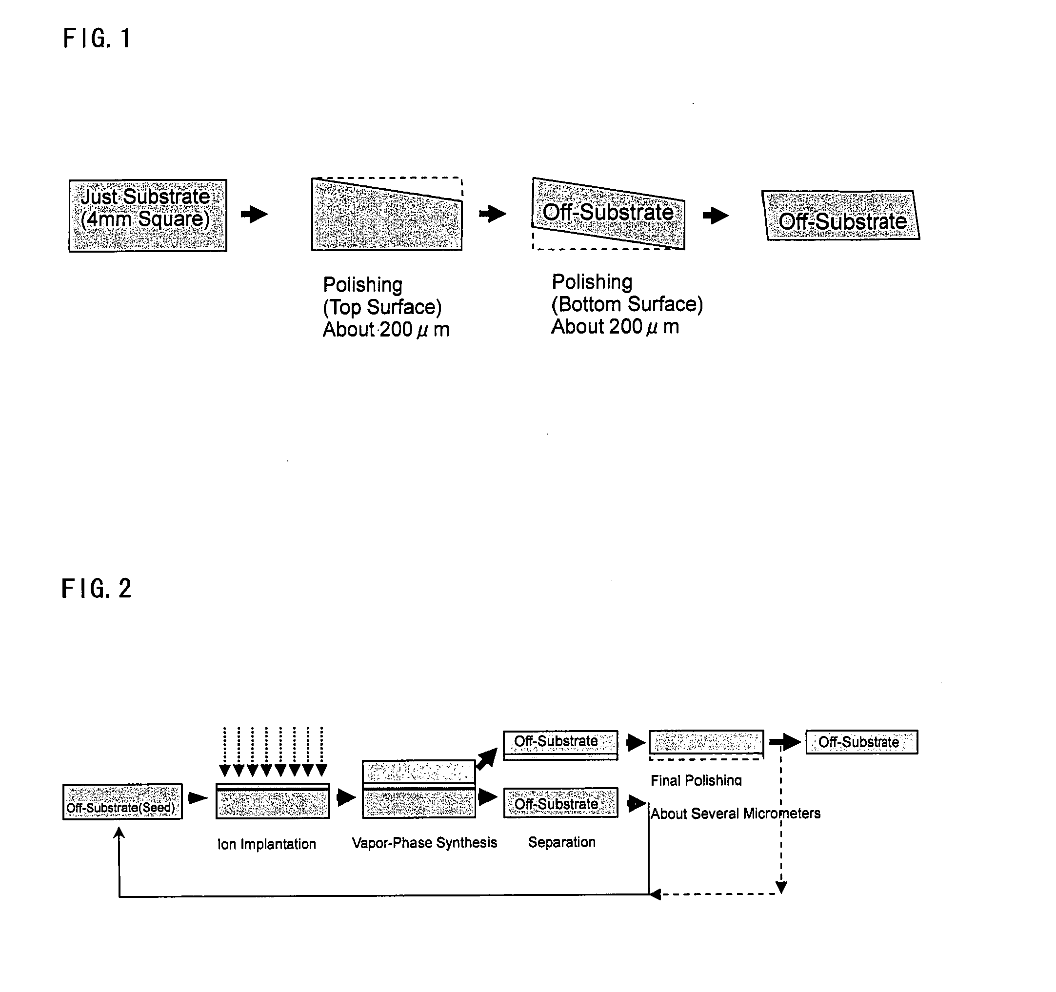
[0050]A high-temperature high-pressure synthetic Ib diamond substrate with a size of 4×4×0.4 mm3, whose surface had been polished to have an off-angle of 3.2° from the (100) plane, was used as a seed crystal (an off-substrate), and diamond growth was performed using a microwave CVD method according to the following method.

[0051]First, carbon ions were implanted into the seed crystal at an implantation energy of 3 MeV and a dose of 2×10¹⁶ ions / cm2 using a 1.5 MV tandem accelerator. The projectile range of the implanted ions was calculated using a Monte Carlo simulation code, and the result was about 1.6 μm. As a result of this irradiation, the color of the diamond substrate changed from a pale yellow to black; this confirmed that a non-diamond layer had been formed.

[0052]The substrate was placed in a commercially available microwave plasma CVD apparatus, and then hydrogen gas was introduced into the CVD chamber, and microwave power was applied to generate plasma. Microwave power was ...

example 2

[0057]A high-temperature high-pressure synthetic Ib diamond substrate with a size of 4×4×0.4 mm3, whose surface had been polished to have an off-angle of 2.6° from the (100) plane, was used as a seed crystal (an off-substrate), and ion implantation and diamond growth by a microwave CVD method were performed according to the same method as Example 1.

[0058]After growing a single-crystal diamond according to the above-described method, the diamond deposited around the ion-implanted layer on the substrate-side surface was removed by laser cutting, and electrochemical etching was performed to separate the diamond growth layer from the substrate, as in Example 1.

[0059]The thickness of the separated diamond growth layer was measured using a micrometer, and the result was 360 μm, which substantially coincided with the growth film thickness. Further, the off-angle of the separated face was measured by X-ray diffraction; as a result, the separated diamond growth layer had an off-angle of 2.5°...


PUM

PropertyMeasurementUnit
off-angleaaaaaaaaaa
off-angleaaaaaaaaaa
energyaaaaaaaaaa

Abstract

The invention provides a process for producing a single-crystal substrate with an off-angle, which comprises using, as a substrate, a material capable of epitaxial growth by a vapor-phase synthesis method, whose surface has an off-angle with respect to a crystal plane capable of epitaxial growth; implanting ions into the substrate having a surface with an off-angle to form a layer with a deteriorated crystal structure near the surface of the substrate; growing a crystal on the surface with an off-angle of the substrate by a vapor-phase synthesis method; and separating a grown crystal layer from the substrate. In accordance with the process of the invention, when producing off-substrates usable in vapor-phase synthesis of single crystals, the manufacturing costs can be reduced, and substrates with an identical off-angle can be produced easily and in large quantities.

Description

TECHNICAL FIELD[0001]The present invention relates to a process for producing a single-crystal substrate with an off-angle that is suitable as a substrate for growing a semiconductor diamond by a vapor-phase synthesis method, or the like.BACKGROUND ART[0002]Diamond, which exhibits outstanding properties as a semiconductor, is expected to be a material for use in semiconductor devices, such as high-frequency and high-output devices, ultraviolet emitting devices, and the like. A single-crystal diamond is grown mainly by methods such as a high-pressure synthesis method, a vapor-phase synthesis method, and the like; a semiconductor-grade, high-quality diamond, in particular, is synthesized by homoepitaxial growth on a diamond substrate using a vapor-phase synthesis method.[0003]However, during the epitaxial growth of a diamond using a vapor-phase synthesis method, many defects such as non-epitaxial crystallites and hillocks tend to occur, and these defects cause electrical properties to...

Claims


Application Information

Patent Timeline
Patent Type & Authority Applications(United States)
IPC IPC(8): C30B23/00
CPCC30B25/00C30B25/02C30B29/04C30B31/22C30B33/00H01L21/02664H01L21/02378H01L21/02381H01L21/02527H01L21/0262H01L21/02658H01L21/02376
Inventor MOKUNO, YOSHIAKICHAYAHARA, AKIYOSHIYAMADA, HIDEAKISHIKATA, SHINICHI
Owner NAT INST OF ADVANCED IND SCI & TECH
Why Eureka
Try Eureka