[0010]Here we propose to use selective area
epitaxy (SAE) to achieve increased-In-content InGaN
layers without changing the MOCVD reactor growth conditions. That is, for the same
growth pressure, temperature, and partial pressures of the In and Ga precursors, the
solid composition of the InGaN film will possess higher In levels. This technique will enable increased temperature growth conditions to avoid the low temperatures conditions commonly used for increased-In-content InGaN) that are known to degrade
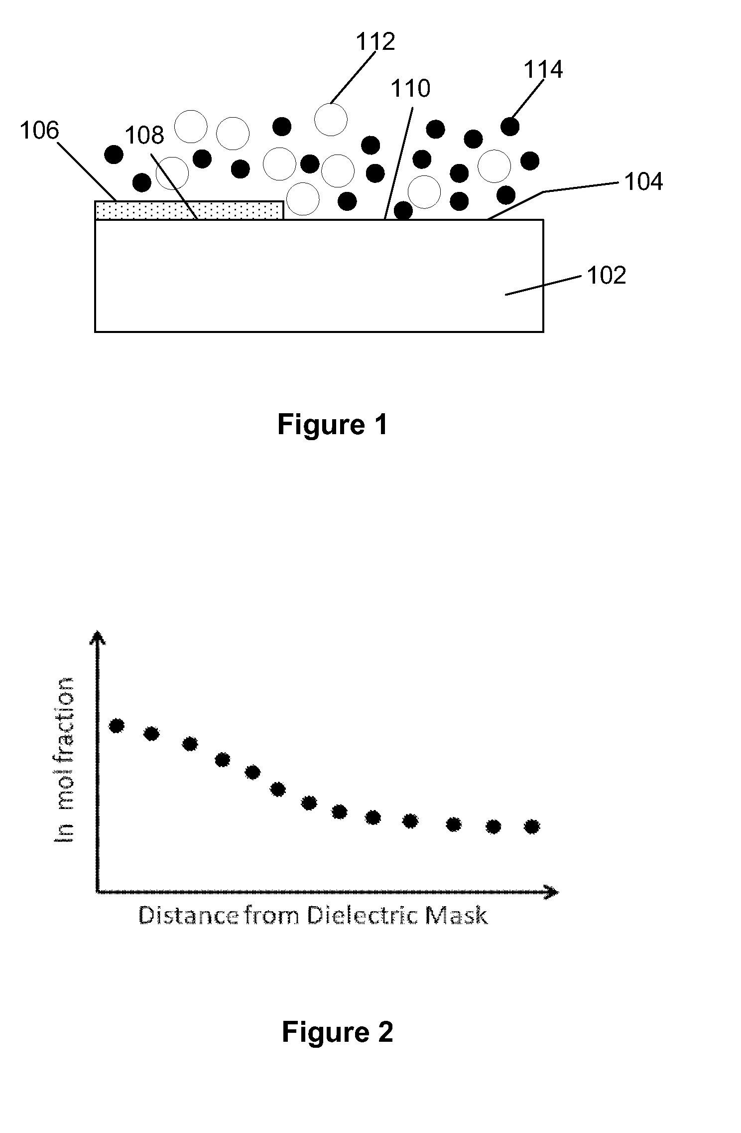
crystal quality. In SAE, a
dielectric (SiO2, SixNy, etc)
mask is deposited on the
substrate surface, lithographically patterned, and then etched such that various geometries of exposed
semiconductor are realized. For
laser diode fabrication the geometry of the unmasked area is often a long (100s of microns) narrow (1-5 microns) stripe. When subjected to epitaxial growth in an MOCVD reactor where the group-III precursors have a
high surface and
gas phase mobility, growth
initiation can be prevented in the masked areas. A growth rate enhancement is observed in the unmasked areas adjacent to the
dielectric mask from the increased concentration of the growth
rate limiting group-III (In and Ga) adatoms within these areas. The lack of depletion of the group-III precursor molecules in the
gas phase over the masked regions coupled with the
high surface mobility of the group-III adatoms on the masked areas leads to an increased concentration of the group-III adatoms present in the growth area adjacent to the
dielectric mask boundary. A key aspect of our invention is that the difference between the
diffusion properties of the In and Ga precursors leads to In-enrichment in the InGaN layer adjacent to the dielectric mask. The metalorganic compounds
trimethylindium (TMIn) and
trimethylgallium (TMGa) are often used as the
source material for In and Ga, respectively. The TMIn molecule decomposes more efficiently than TMGa in the high temperature MOCVD growth conditions, leading to a reduced
average size of the In containing metalorganic molecules. Since the gas-
phase diffusion coefficient increases with reduced molecule size, the In precursors will have a higher diffusivity and will therefore more readily arrive in the growth areas. The result is a relatively higher In content in the In and Ga containing layer (i.e. InGaN) adjacent to the dielectric mask for a given set of reactor conditions. The
kinetics of SAE are a well understood phenomenon in traditional alloys such as InGaAs and InGaAsP [2]. Literature reports similar phenomenon on polar GaN, where researchers have grown InGaN
quantum dots and multi-color LEDs using SAE.
[0011]In our invention, we will employ SAE to overcome the formidable challenge of realizing high-In-content InGaN
quantum wells for the fabrication of high-efficiency
laser diodes and LEDs with extended wavelengths beyond 450 nm into the blue, green, yellow and red regimes. Our implementation of SAE will facilitate increased In incorporation in the In containing layer such as InGaN
quantum wells adjacent to the masked region under identical growth conditions. This technique will be executed on nonpolar and / or semipolar GaN substrates to facilitate high-efficiency long-
wavelength laser diodes and LEDs. Lasers and LEDs fabricated on conventional polar (c-plane) GaN suffer from internal piezoelectric and
spontaneous polarization fields that intrinsically reduce the radiative recombination efficiency of
electron-hole pairs and limit the device performance [3,4]. Early demonstrations of laser diodes fabricated on nonpolar (m-plane) GaN substrates operating at 405 nm and 451.8 nm show great promise for enhanced device performance [5, 6]. Furthermore, high-power green (516 nm) light emitting diodes (LED) fabricated on semipolar substrates indicate a natural tendency for increased In-incorporation on these crystallographic planes [7]. By
coupling this enhanced In-incorporation behavior with minimized internal piezoelectric and spontaneous fields on semipolar substrates with our proposed SAE method for increased In-incorporation, our invention will enable the fabrication of high-efficiency blue, green, yellow and red emitting laser diodes and LEDs.
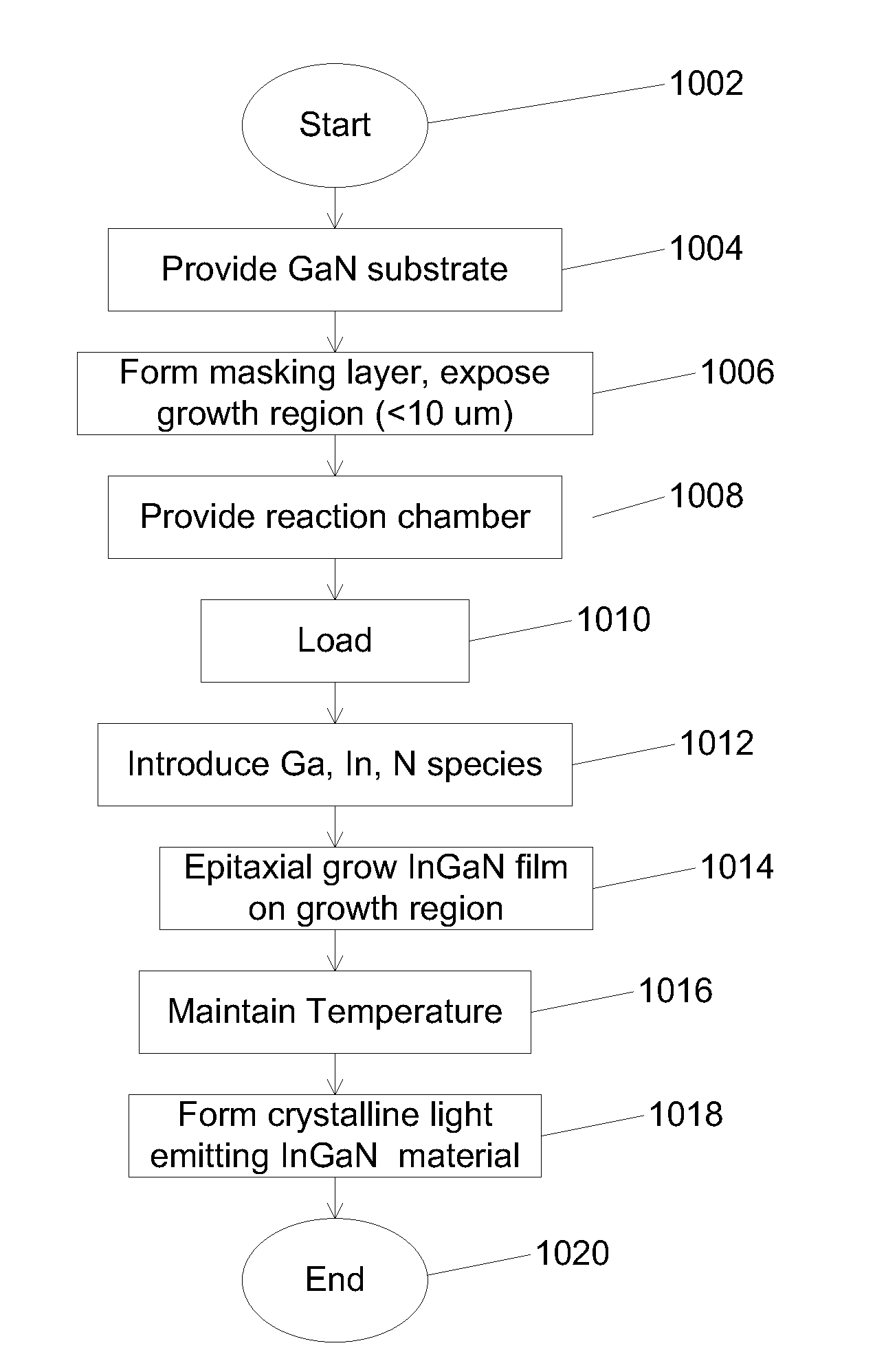
[0012]
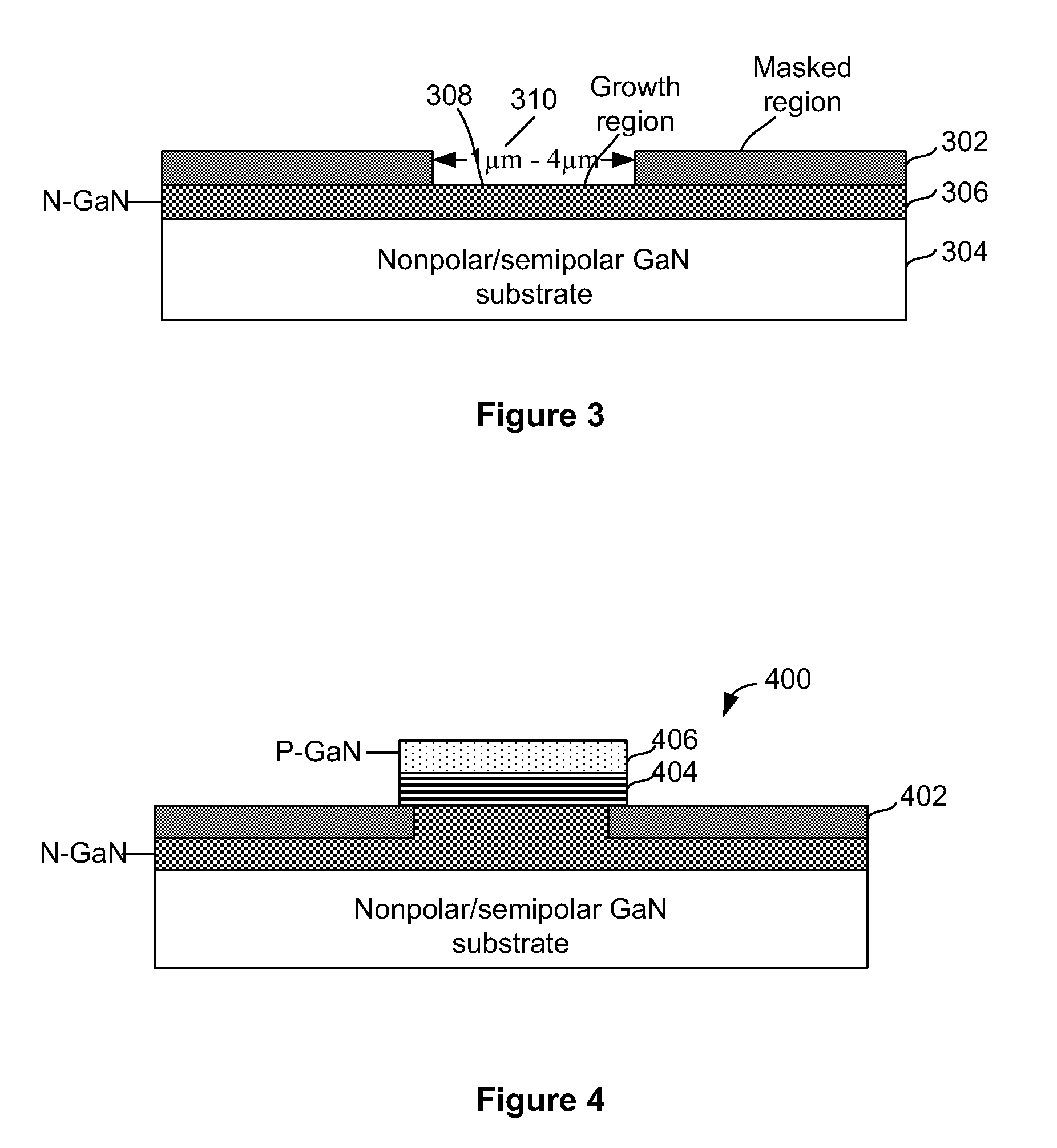
Laser diodes will be fabricated by patterning a dielectric mask either directly on the nonpolar / semipolar substrate or on an n-doped layer grown on the said substrates to form narrow stripes of unmasked growth area. The wafers will then be subjected to MOCVD growth where growth will initiate with an n-type GaN cladding layer, followed by the active region containing In containing quantum wells such as InGaN. The growth of the InGaN quantum wells in these narrow unmasked stripe areas will result in high-In-content quantum wells based on the SAE
kinetics discussed above, pushing the emission
wavelength to values required for blue, green, yellow and red emission. After deposition of the active region
layers, the growth can be continued to deposit the p-GaN upper cladding layer or the growth can be interrupted. In the latter case, the sample would be removed from the reactor, the dielectric mask selectively etched, and the sample would be subjected to a regrowth for the definition of the p-cladding layer to realize a buried stripe laser structure. In the former case, where the p-cladding is defined in the same growth as the active region, surface
ridge laser architectures could be easily fabricated from the resulting epitaxial structure.
[0021]Other benefits are achieved over conventional techniques. For example, the
present method and device achieves high brightness and
high resolution lighting technologies that require blue, green, yellow or red contributions such as
high resolution red-green-blue displays, communications in
polymer-based fibers, or
solid-state lighting based on red-green-blue or blue-
yellow laser diodes and LEDs. In a specific embodiment, the present invention provides improved
crystal quality, highly efficient laser diodes and LEDs on nonpolar / semipolar. GaN will enable laser and LED emission in the blue, green, yellow and red bands, allowing the realization of true color displays based on red-green-blue or blue-
yellow laser diodes. In a preferred embodiment, the absence of polarization fields in the quantum wells on the substrates along with the increased growth temperatures enabled by SAE will facilitate high efficiency device operation. Thus, this technology would allow for the improvement of existing devices such as 405 nm lasers used in HD-DVD and Sony Blue-
Ray along with completely new technologies demanding blue, green, yellow and red emission and low
power consumption.

