Process for forming a ceramic oxide material with a pyrochlore structure having a high dielectric constant and implementation of this process for applications in microelectronics

a technology of pyrochlore structure and ceramic oxide material, which is applied in the direction of electrolytic capacitors, chemical vapor deposition coatings, ion implantation coatings, etc., can solve the problems of high dielectric loss, degrading surrounding components and interconnections, etc., and achieves high dielectric constant, low thermal dissipation factor, and advantageous dielectric properties.

Active Publication Date: 2010-03-25
COMMISSARIAT A LENERGIE ATOMIQUE ET AUX ENERGIES ALTERNATIVES
View PDF11 Cites 2 Cited by
  • Summary
  • Abstract
  • Description
  • Claims
  • Application Information

AI Technical Summary

Benefits of technology

[0017]Thus, the present inventors have discovered, surprisingly, that by working within a certain annealing temperature range, starting from a particular base material, it is possible to obtain materials that crystallize in the pyrochlore system and have particularly advantageous dielectric properties, such as a high dielectric constant and a low thermal dissipation factor.

Problems solved by technology

However, this dielectric material has a number of drawbacks, among which that may be mentioned is a low dielectric constant of around 3.9.
To obtain capacitance values necessary for circuits to operate correctly, capacitors using silicon dioxide as dielectric material must, in order to compensate for the relatively low dielectric constant, have a very large area and indeed a very small thickness, this being incompatible with the wish to obtain a high density of capacitive components in integrated circuits.
What is more, by reducing the thickness of the SiO2 layers, high tunnel currents may appear, these being prejudicial to correct operation of the integrated circuits in which the capacitors are included.
These materials have, advantageously, a very high dielectric constant (of the order of 1000) but, however, a dielectric loss that is also high (around 0.02-0.05), which may prove to be problematic in certain microelectronic applications.
However, the formation of such materials requires working at temperatures often above 550° C. Such temperatures may be deleterious, especially when the materials are intended to be produced on integrated circuits, such temperature levels possibly degrading the surrounding components and the interconnects.

Method used


Image

  • Process for forming a ceramic oxide material with a pyrochlore structure having a high dielectric constant and implementation of this process for applications in microelectronics
  • Process for forming a ceramic oxide material with a pyrochlore structure having a high dielectric constant and implementation of this process for applications in microelectronics
  • Process for forming a ceramic oxide material with a pyrochlore structure having a high dielectric constant and implementation of this process for applications in microelectronics

Examples


example

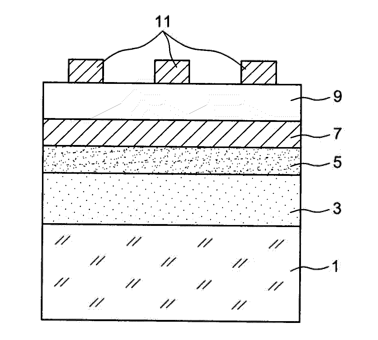
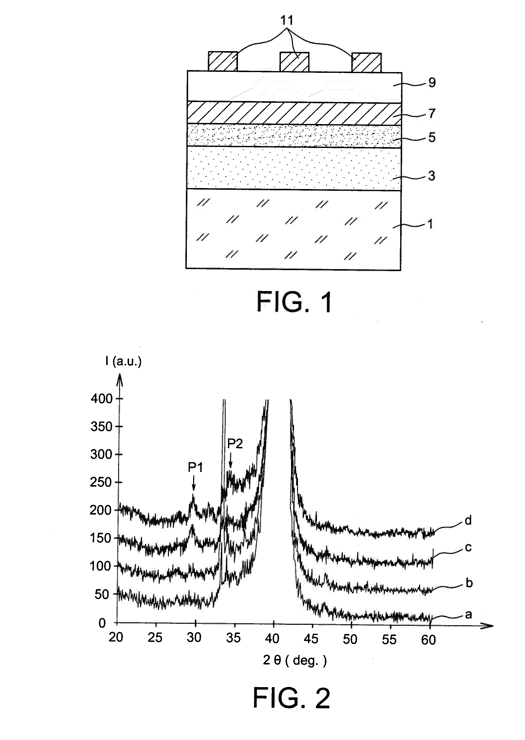
[0084]Deposited on a multilayer stack comprising, as illustrated in FIG. 1:

[0085]a silicon wafer 1;

[0086]an SiO2 silica layer 3 about 0.5 μm in thickness;

[0087]a titanium dioxide TiO2 layer 5 about 20 nm in thickness; and

[0088]a platinum Pt layer 7 about 100 nm in thickness,

[0089]was an amorphous ceramic oxide layer 9 having the nominal composition 0.9Pb(Mg1 / 3Nb2 / 3)O3-0.1PbTiO3 9 (the sputtering target having been purchased from the supplier Super Conductor Materials, Inc., USA) with 15% excess MgO by magnetron sputtering with argon as plasma gas.

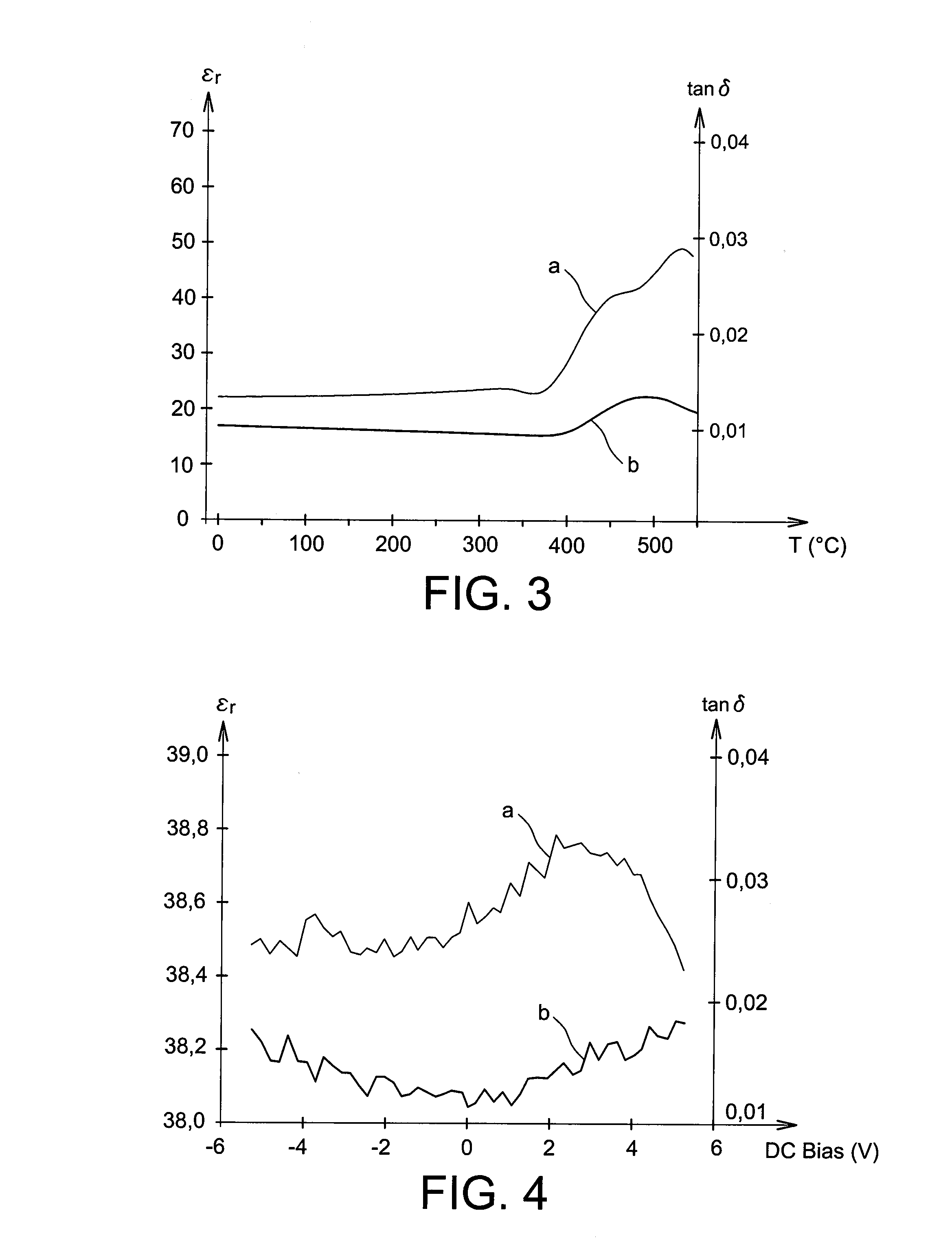
[0090]The resulting multilayer stack was then heated at various annealing temperatures, stretching from room temperature, 300, 350, 400, 450° C., 500 and 550° C., in a conventional air oven.

[0091]The ceramic oxide layer had a thickness of about 50 nm.

[0092]To determine the electrical and dielectric properties of the ceramic oxide layer deposited, circular platinum electrodes 11 with a diameter of 110 μm were deposited on the surface of said...


PUM

PropertyMeasurementUnit
temperatureaaaaaaaaaa

Abstract

The invention relates to a process for forming a lead-based ceramic oxide dielectric material comprising at least one pyrochlore crystalline phase, which process comprises the following steps: a) a step of depositing at least one amorphous layer of said lead-based ceramic oxide material on a substrate; and b) a crystallization annealing step carried out on said amorphous layer at a temperature not exceeding 550° C., by means of which a lead-based ceramic oxide dielectric material comprising at least one pyrochlore phase is obtained. Application to the fabrication of capacitors on integrated circuits.

Description

CROSS REFERENCE TO RELATED APPLICATIONS or PRIORITY CLAIM[0001]This application claims priority of French Patent Application No. 08 56386, filed Sep. 23, 2008.DESCRIPTION[0002]1Technical Field[0003]The present invention relates to a process for forming a lead-based ceramic oxide material with a pyrochlore structure, this material advantageously having a dielectric loss ≦0.015 and a dielectric constant ≧40.[0004]This process is applicable, in particular, in the fabrication of passive components, especially in the design of capacitors comprising a dielectric part capable of storing a large amount of electric charge per unit area, it being possible for these components to be placed on the surface of integrated circuits, thus corresponding to the “above IC” approach). This process is also applicable in the fabrication of “stand-alone” components (i.e. corresponding to components produced on a substrate independent of that of the integrated circuits with which they are associated).[0005]...

Claims


Application Information

Patent Timeline
Patent Type & Authority Applications(United States)
IPC IPC(8): H01G9/00B05D3/02C23C16/44C23C14/34C23C14/35
CPCH01G4/12C23C14/088C23C14/56C23C14/5806C23C14/584
Inventor ZHU, XIAOHONGDEFAY, EMMANUELFRIBOURG-BLANC, ERIC
Owner COMMISSARIAT A LENERGIE ATOMIQUE ET AUX ENERGIES ALTERNATIVES
Why Eureka
Try Eureka