Metal oxide-containing film-forming composition, metal oxide-containing film-formed substrate, and patterning process

a metal oxide-containing film and composition technology, applied in the direction of photosensitive materials, instruments, photomechanical equipment, etc., can solve the problems of deteriorating resolution performance of photoresist film, pattern collapse, and inability to accurately transfer resist pattern onto processing substrate, etc., to achieve excellent dry etching characteristic and excellent storage stability

Active Publication Date: 2010-04-08
SHIN ETSU CHEM IND CO LTD
View PDF24 Cites 68 Cited by
  • Summary
  • Abstract
  • Description
  • Claims
  • Application Information

AI Technical Summary

Benefits of technology

[0032]The present invention has been carried out in view of the above circumstances, and it is therefore an object of the present invention to provide: a metal oxide-containing film-forming composition for forming a metal oxide-containing film, such that: (1) the film mad of the composition allows for formation of an excellent resist film pattern even under a high-NA exposure condition, when the photoresist film is formed as a resist upper layer film on the metal oxide-containing film formed on an organic film acting as a resist lower layer film, and the resist film pattern is subsequently formed; (2) the film made of the composition has an excellent dry etching characteristic relative to the photoresist film and the organic film; (3) the composition is excellent in storage stability; and (4) the film made of the composition is capable of being delaminated, not only by conventional hydrofluoric acid, dry delamination, and the like, but also by a solution used in a delamination process such as a sulfuric acid-hydrogen peroxide-water mixture, ammonia-hydrogen peroxide-water mixture, or the like; a substrate formed with a metal oxide-containing film formed from the metal oxide-containing film-forming composition; and a patterning process using the composition.

Problems solved by technology

However, when a pattern is made finer, i.e., pattern rules are further narrowed while keeping a thickness of a used photoresist film as it is, the photoresist film is deteriorated in resolution performance.
Further, when the resist film is to be developed by a developer to form a pattern, a so-called aspect ratio thereof is made excessively large, thereby resultingly causing a pattern collapse.
Meanwhile, although for processing of a processing substrate, there is typically used a method for processing the processing substrate by dry etching by adopting a patterned photoresist film as an etching mask, practically no dry etching methods exist to exhibit a complete etching selectivity between a photoresist film and a processing substrate, so that the resist film is also damaged during processing of the processing substrate and the resist film is collapsed, thereby failing to accurately transfer a resist pattern onto the processing substrate.
However, etching speeds under the dry etching condition have been practically made higher, so that recent photoresist compositions having higher resolutions practically tend to be rather lowered in etching resistance.
Since such a pattern transference based on dry etching leads to obtainment of a transferred pattern in a relatively excellent profile when an etching resistance of the etching mask is sufficient, problems are scarcely caused such as pattern collapse due to friction or the like by a developer upon development of a resist, thereby allowing for obtainment of a pattern having a relatively large aspect ratio.
In a via-first method which is one of substrate processing methods where a processing intermediate substrate has large height differences, an attempt to form a pattern with a single resist film encounters a problem such as inaccurate focusing during resist exposure due to a substantial difference in resist film thickness.
Silicon-containing films having been conventionally used in such a multi-layer resist process have several problems.
As such, the overlying photoresist film is subjected to an additional burden of dry etching to an extent the processing of the organic antireflective film.
Particularly, most-advanced photoresist films have been made small in thickness, so that such dry etching burden is not negligible.
However, since the aromatic ring structure for effective light absorption has a function to lower a dry etching speed in case of dry etching by fluorine-based gas plasma, this is a disadvantageous way to conduct dry etching of a resist intermediate film without burdening a photoresist film.
Then, since addition of a large amount of such light-absorbing substitutional groups is undesirable, it is required to restrict the addition amount to a minimum.
However, since no descriptions are found concerning a light-absorbing group for the disclosed composition, it is supposed that a silicon-containing film to be obtained from the composition fails to have an antireflective function.
This fails to prevent reflection upon exposure in lithography using a most-advanced high-NA exposure system, thereby possibly failing to obtain a finer resist pattern profile.
Moreover, since photoresist films have been further decreased in thickness in a most-advanced semiconductor process using the above-described high-NA exposure system, it is predicted that a pattern transference to a silicon-containing intermediate film is made difficult in case of etching the intermediate film by using a photoresist film as an etching mask, when a silicon content of the silicon-containing intermediate film is merely increased while possessing an antireflective function.
Moreover, such a condensation reaction occasionally progresses endlessly, to an extent that the silicon-containing compound solution is eventually gelated.
Since fluctuation of lithography performance is particularly delicate, such a fluctuation is inevitably observed as a change of finer pattern profile even when condensation of silanol groups in molecules is not observable as a film thickness increase or a molecular weight change.
However, even when such countermeasures are taken for silicon-containing compounds in silicon-containing film-forming compositions produced in the above methods, it is actually impossible to completely stop condensation reactions of silanol groups, so that the silicon-containing compounds slowly change over time, and natures of silicon-containing films to be obtained from the thus changed silicon-containing film-forming compositions are also changed.
Meanwhile, in an actual manufacturing process of a semiconductor device, defects are occasionally caused in coated films formed on the substrate, and re-processing is thus to be performed.
Thus, to remove the films, dry delamination or the like based on hydrofluoric acid or fluorine gas has been conducted, but such a removal technique has brought about a serious damage against the substrate.

Method used


Image

  • Metal oxide-containing film-forming composition, metal oxide-containing film-formed substrate, and patterning process
  • Metal oxide-containing film-forming composition, metal oxide-containing film-formed substrate, and patterning process
  • Metal oxide-containing film-forming composition, metal oxide-containing film-formed substrate, and patterning process

Examples


synthesis example 1

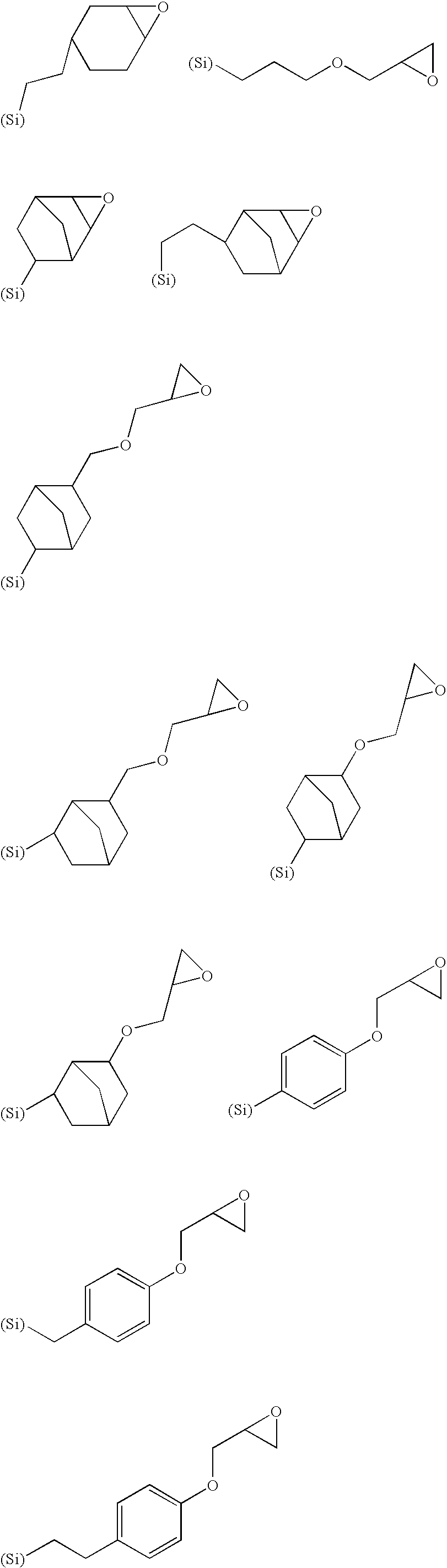
[0380]Added into a mixture of 40 g of propylene glycol methyl ether, 1 g of methanesulfonic acid, and 50 g of deionized water, was a mixture of 10 g of phenyltrimethoxysilane, 20 g of 2-(3,4-epoxycyclohexyl)ethyltrimethoxysilane, 10 g of tetrabutoxy germanium, and 35 g of propylene glycol methyl ether; the resultant mixture was kept as it was for 12 hours at 40° C. to thereby subject it to hydrolytic condensation; and then by-product alcohols were distilledly removed therefrom under reduced pressure. Added to the resultant mixture were 800 ml of ethyl acetate and 300 ml of propylene glycol methyl ether, and a water layer was separated from the resultant mixture. Added to the remaining organic layer was 100 ml of ion exchange water, followed by stirring, still standing, and separation. This was repeated three times. Added to the remaining organic layer was 200 ml of propylene glycol methyl ether, followed by concentration thereof under reduced pressure, thereby obtaining 100 g of a p...

synthesis example 2

[0381]Added into a mixture of 40 g of propylene glycol methyl ether, 1 g of methanesulfonic acid, and 50 g of deionized water, was a mixture of 10 g of phenyltrimethoxysilane, 20 g of 2-(3,4-epoxycyclohexyl)ethyltrimethoxysilane, 10 g of tetrabutoxy titanium, 20 g of 2,4-pentanedione, and 35 g of propylene glycol methyl ether; the resultant mixture was kept as it was for 12 hours at 30° C. to thereby subject it to hydrolytic condensation; and then by-product alcohols were distilledly removed therefrom under reduced pressure. Added to the remaining solution was 200 ml of propylene glycol methyl ether, followed by concentration thereof under reduced pressure, thereby obtaining 120 g of a propylene glycol methyl ether solution (polymer concentration of 20%) of a metal oxide-containing compound 2. The polymer was measured for a molecular weight, and determined to have Mw=8,000 relative to polystyrene standards.

synthesis example 3

[0382]Added into a mixture of 40 g of propylene glycol ethyl ether, 1 g of hydrochloric acid, and 50 g of deionized water, was a mixture of 10 g of phenyltrimethoxysilane, 20 g of 2-(3,4-epoxycyclohexyl)ethyltrimethoxysilane, 10 g of tetrapropoxy hafnium, and 35 g of propylene glycol ethyl ether; the resultant mixture was kept as it was for 12 hours at 10° C. to thereby subject it to hydrolytic condensation; and then by-product alcohols were distilledly removed therefrom under reduced pressure. Added to the remaining solution was 200 ml of propylene glycol ethyl ether, followed by concentration thereof under reduced pressure, thereby obtaining 100 g of a propylene glycol ethyl ether solution (polymer concentration of 20%) of a metal oxide-containing compound 3. The polymer was measured for a molecular weight, and determined to have Mw=5,000 relative to polystyrene standards.


PUM

PropertyMeasurementUnit
wavelengthaaaaaaaaaa
temperatureaaaaaaaaaa
hydrolyzableaaaaaaaaaa

Abstract

There is disclosed a thermosetting metal oxide-containing film-forming composition for forming a metal oxide-containing film to be formed in a multilayer resist process used in lithography, the thermosetting metal oxide-containing film-forming composition comprising, at least: (A) a metal oxide-containing compound obtained by hydrolytic condensation of a hydrolyzable silicon compound and a hydrolyzable metal compound; (B) a thermal crosslinking accelerator; (C) a monovalent, divalent, or higher organic acid having 1 to 30 carbon atoms; (D) a trivalent or higher alcohol; and (E) an organic solvent. There can be provided a metal oxide-containing film-forming composition in a multi-layer resist process, in a manner that a film made of the composition allows for formation of an excellent pattern of a photoresist film, the composition is capable of forming a metal oxide-containing film as an etching mask having an excellent dry etching resistance, the composition is excellent in storage stability, and the film made of the composition is removable by a solution used in a removal process; a metal oxide-containing film-formed substrate; and a pattern forming process.

Description

BACKGROUND OF THE INVENTION[0001]1. Field of the Invention[0002]The present invention relates to a metal oxide-containing film-forming composition for forming a metal oxide-containing film to be used in a multi-layer resist process used for fine processing in a manufacturing process of semiconductor devices and the like; a metal oxide-containing film-formed substrate; and a patterning process using the composition.[0003]2. Description of the Related Art[0004]With highly integrated LSI's providing highly increased speeds, finer pattern rules are being rapidly promoted. Commensurately with the fineness, the lithography technique has attained formation of fine patterns, by virtue of light sources of shorter wavelengths and resist compositions appropriately selected therefor. The main role thereof was played by positive photoresist compositions to be each used as a monolayer. The monolayer positive photoresist composition is configured to possess, in a resist resin, a frame having an et...

Claims


Application Information

Patent Timeline
Patent Type & Authority Applications(United States)
IPC IPC(8): G03F7/00
CPCC08G77/58G03F7/11G03F7/0752C09D183/04G03F7/039G03F7/075G03F7/09
Inventor OGIHARA, TSUTOMUUEDA, TAKAFUMIYANO, TOSHIHARU
Owner SHIN ETSU CHEM IND CO LTD
Why Eureka
Try Eureka