Method for manufacturing soi substrate

a technology of silicon-based substrates and soi, which is applied in the direction of basic electric elements, electrical equipment, semiconductor devices, etc., can solve the problems that the recovery of crystallinity and planarization of single crystal silicon layers cannot be carried out by such a method, and the surface of the single crystal silicon layer over the soi substrate has crystal defects and loses its planarity, so as to achieve the effect of improving the planarity, reducing the deficiency region, and improving the planar

Inactive Publication Date: 2010-04-08
SEMICON ENERGY LAB CO LTD
View PDF73 Cites 20 Cited by
  • Summary
  • Abstract
  • Description
  • Claims
  • Application Information

AI Technical Summary

Benefits of technology

[0019]In accordance with one embodiment of the present invention, by irradiating a single crystal semiconductor film over an SOI substrate with laser light, crystal defects of the single crystal semiconductor film over the glass substrate can be repaired and planarity of the single crystal semiconductor film can be improved. Moreover, the dose of hydrogen ions in the formation of an embrittled layer is set to a dose 2.2 times or more as high as the lower limit of the dose of hydrogen ions for separat

Problems solved by technology

The surface of the single crystal silicon layer over an SOI substrate manufactured by a Smart Cut method has crystal defects and loses its planarity due to ion introduction for forming an embrittled layer (the hydrogen ion implanted plane) and separation of a single crystal silicon substrate (a bond substrate) by heat treatment.
Moreover, crystal defects in the single crystal silicon layer cause an adverse effect on electrical characteristics of a semiconductor element.
On the other

Method used


Image

  • Method for manufacturing soi substrate
  • Method for manufacturing soi substrate
  • Method for manufacturing soi substrate

Examples


embodiment 1

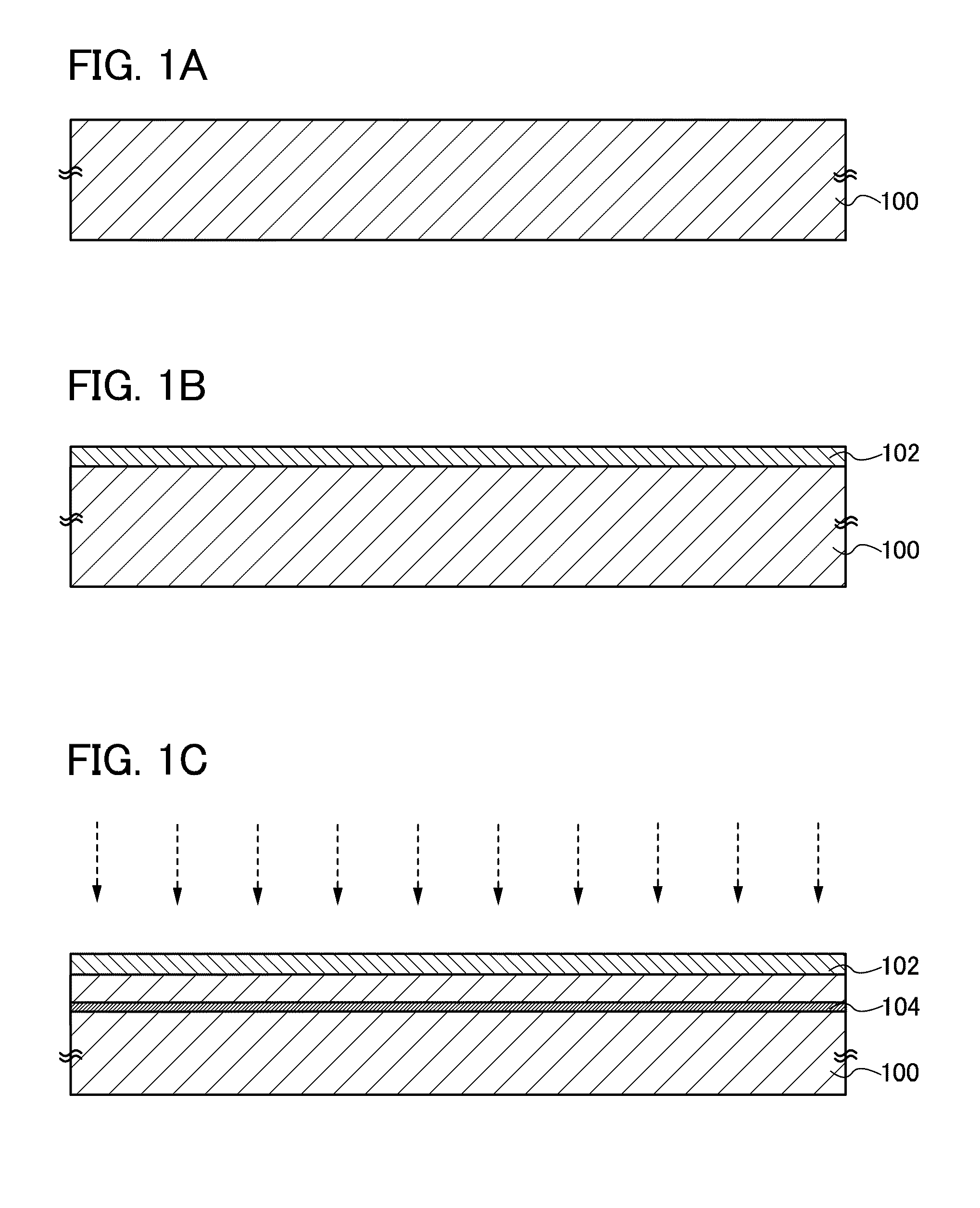
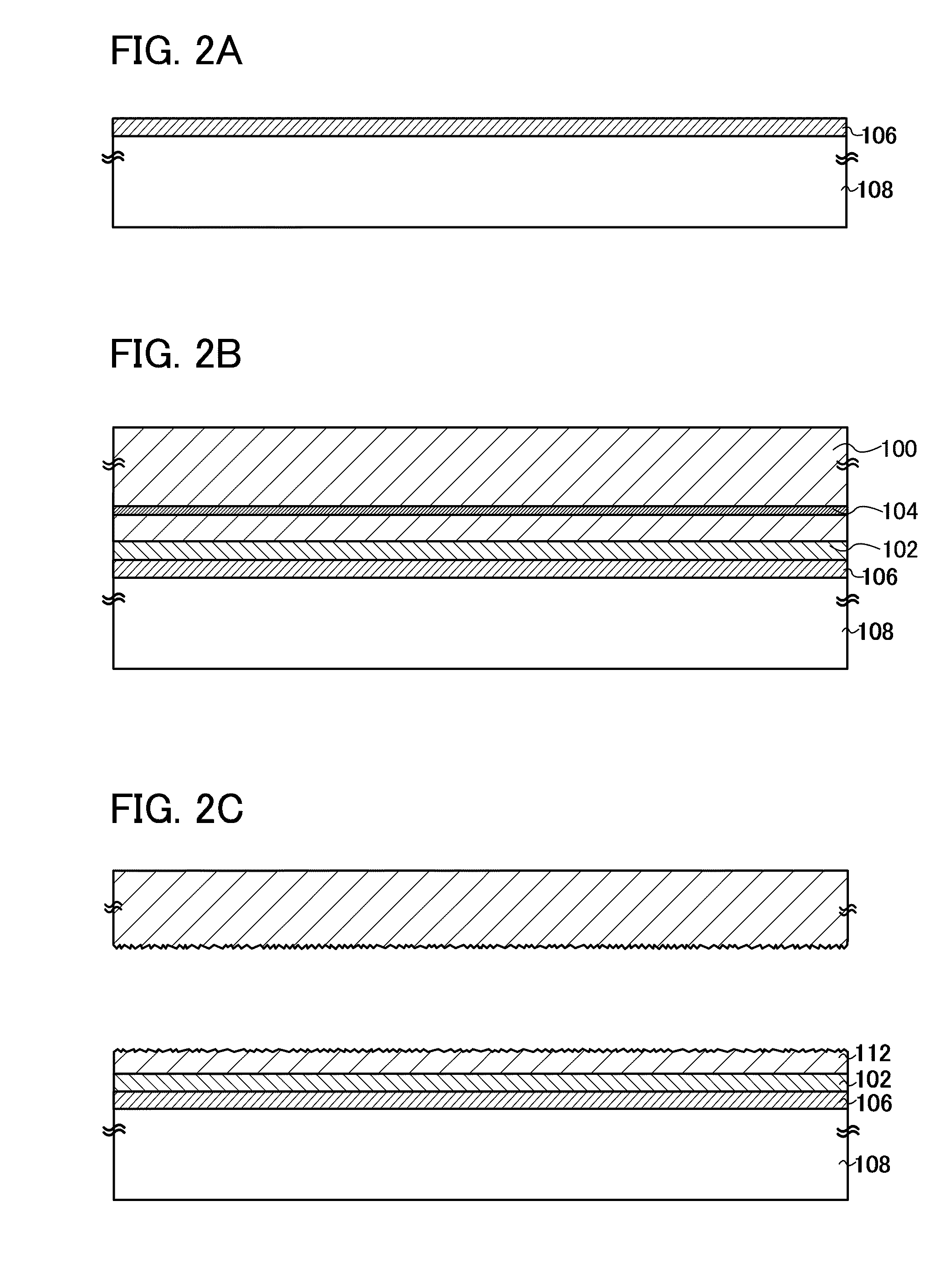
[0041]In a method for manufacturing an SOI substrate according to this embodiment, an SOI substrate is manufactured by attaching a semiconductor film separated from a semiconductor substrate which serves as a bond substrate to a base substrate. A method for manufacturing an SOI substrate according to this embodiment is described below with reference to FIGS. 1A to 1C, FIGS. 2A to 2C, and FIGS. 3A to 3C.

[0042]First, a bond substrate 100 illustrated in FIG. 1A is prepared. As the bond substrate 100, a commercially available semiconductor substrate, for example, a single crystal semiconductor substrate formed of silicon, germanium, or the like or a polycrystalline semiconductor substrate formed of silicon, germanium, or the like can be used. Alternatively, a single crystal semiconductor substrate formed of a compound semiconductor such as gallium arsenide or indium phosphide or a polycrystalline semiconductor substrate formed of a compound semiconductor such as gallium arsenide or indi...

embodiment 2

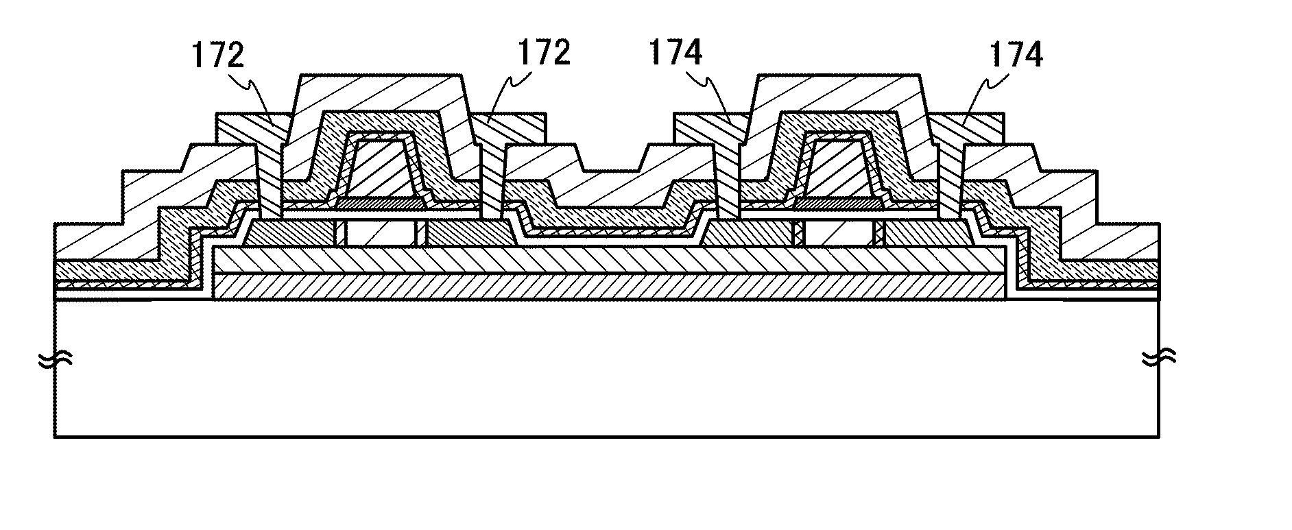
[0118]In this embodiment, a semiconductor device is manufactured using the SOI substrate manufactured in Embodiment 1. A method for manufacturing an n-channel thin film transistor and a p-channel thin film transistor is described with reference to FIGS. 4A to 4D, FIGS. 5A to 5C, and FIGS. 6A to 6C. By combining a plurality of thin film transistors (TFTs), various types of semiconductor devices can be manufactured.

[0119]First, a p-type impurity element such as boron, aluminum, or gallium or an n-type impurity element such as phosphorus or arsenic is preferably added to the semiconductor film 112 in accordance with a formation region of an n-channel thin film transistor or a p-channel thin film transistor. For example, a p-type impurity element is added to a formation region of an n-channel thin film transistor and an n-type impurity element is added to a formation region of a p-channel thin film transistor, whereby so-called well regions are formed. The dose of impurity ions may be a...

embodiment 3

[0154]In this embodiment, a method for manufacturing a semiconductor device in which sidewalls are formed differently from Embodiment 2 to form high-concentration impurity regions, low-concentration impurity regions, and a channel formation region in a semiconductor film is described with reference to FIGS. 7A to 7D.

[0155]First, in a manner similar to that of Embodiment 1, the insulating film 106, the insulating film 102, the semiconductor film 116, and the semiconductor film 118 are formed over the base substrate 108 and they are covered with the gate insulating film 120, the first conductive film 122, and the second conductive film 124 as illustrated in FIG. 4C.

[0156]Next, the resist mask 126 and the resist mask 128 are selectively formed over the second conductive film 124. Then, the first conductive film 122 and the second conductive film 124 are etched using the resist mask 126 and the resist mask 128. Accordingly, a gate electrode 208 with a two-layer structure formed using a ...


PUM


Abstract

An SOI substrate is manufactured by forming an embrittled layer in a bond substrate by increasing the dose of hydrogen ions in the formation of the embrittled layer to a value more than the dose of hydrogen ions of the lower limit for separation of the bond substrate, separating the bond substrate attached to the base substrate, forming an SOI substrate in which a single crystal semiconductor film is formed over the base substrate, and irradiating a surface of the single crystal semiconductor film with laser light.

Description

BACKGROUND OF THE INVENTION[0001]1. Field of the Invention[0002]The present invention relates to a method for manufacturing a substrate provided with a semiconductor layer with an insulating film interposed therebetween, particularly, a silicon-on-insulator (SOI) substrate.[0003]2. Description of the Related Art[0004]In recent years, integrated circuits which use a silicon-on-insulator (SOI) substrate in which a thin single crystal semiconductor layer is provided over an insulating surface, instead of a bulk silicon wafer, have developed. By utilizing characteristics of a thin single crystal silicon film formed over an insulating film, transistors formed in the integrated circuit can be separated from each other completely. Further, since fully-depleted transistors can be formed, a semiconductor integrated circuit with high added value such as high integration, high speed driving, and low power consumption can be realized.[0005]One of known methods for manufacturing an SOI substrate...

Claims


Application Information

Patent Timeline
IPC IPC(8): H01L21/762H01L21/46
CPCH01L21/76254H01L27/1218H01L29/66772
Inventor SHIMOMURA, AKIHISATOKUNAGA, HAJIME
Owner SEMICON ENERGY LAB CO LTD
Why Eureka
Try Eureka