Solid-state image device, method for producing the same, and image pickup apparatus

a solid-state image and image technology, applied in the direction of television system, final product manufacturing, sustainable manufacturing/processing, etc., can solve the problems of color reproduction, color artifacts, and significant so as to suppress the occurrence of dark current and suppress the reduction of image quality , the effect of high sensitivity

Inactive Publication Date: 2010-07-22
SONY CORP
View PDF10 Cites 21 Cited by
  • Summary
  • Abstract
  • Description
  • Claims
  • Application Information

AI Technical Summary

Benefits of technology

[0020]It is desirable to reduce the pixel size as the number of pixels is increased, achieve high-speed capture, and capture images in a dark place, and prevent a reduction in sensitivity due to a reduction in the number of photons incident on one pixel.
[0021]According to an embodiment of the present invention, there is provided a high-sensitivity solid-state image device including a photoelectric conversion layer having good crystallinity and a high optical absorption coefficient while the occurrence of dark current is suppressed.
[0023]The solid-state image device according to an embodiment of the present invention includes the silicon substrate and the photoelectric conversion layer arranged on the silicon substrate and lattice-matched to the silicon substrate, the photoelectric conversion layer being composed of the chalcopyrite-based compound semiconductor of the CuAlGaInSSe-based mixed crystal or the CuAlGaInZnSSe-based mixed crystal. Thus, the occurrence of dark current is suppressed, and the sensitivity is increased. Hence, an image with excellent image quality and high sensitivity is advantageously obtained.
[0025]In the method for producing a solid-state image device according to an embodiment of the present invention, the photoelectric conversion layer is formed on the silicon substrate while maintaining lattice matching to the silicon substrate, the photoelectric conversion layer being composed of the chalcopyrite-based compound semiconductor of the CuAlGaInSSe-based mixed crystal or the CuAlGaInZnSSe-based mixed crystal. Thus, the occurrence of dark current is suppressed, and the sensitivity is increased. Hence, an image with excellent image quality and high sensitivity is advantageously obtained.
[0027]In the image pickup apparatus according to an embodiment of the present invention, the solid-state image device includes the photoelectric conversion layer arranged on the silicon substrate and lattice-matched to the silicon substrate, the photoelectric conversion layer being composed of the chalcopyrite-based compound semiconductor of the CuAlGaInSSe-based mixed crystal or the CuAlGaInZnSSe-based mixed crystal. Thus, the occurrence of dark current is suppressed, suppressing a reduction in image quality due to bright defects. Furthermore, the solid-state image device has high sensitivity and captures an image with high sensitivity. Hence, capturing an image with high sensitivity and suppressing the reduction in image quality advantageously make it possible to capture an image with high quality even in a dark environment, e.g., in the nighttime.

Problems solved by technology

Thus, demosaicing, which is arithmetic processing to interpolate the color of a pixel from pixels surrounding the pixel, is performed, thereby disadvantageously leading to color artifacts.
However, the photoelectric conversion layer is basically grown on an electrode and is polycrystalline, thus leading to a significant occurrence of dark current due to crystal defects.
This method provides a high degree of color mixing and poor color reproducibility.
Thus, even in the case where a blue signal is not present, the passage of green and red signals leads to the misdetection of a blue signal, causing aliasing and difficulty in providing sufficient color reproducibility.
Thus, a circuit for the calculation is arranged, increasing the complexity and scale of the circuit structure by the circuit and leading to an increase in cost.
Furthermore, if one of the three primary colors is saturated, the true value of the signal of the saturated color is not determined, thereby leading to miscalculation.
That is, the method is not suitable for a reduction in pixel size.
In the case where materials having different crystal structures are bonded to each other, a difference in lattice constant causes misfit dislocation, reducing crystallinity.
As a result, electrons trapped at a defect level formed in the band gap are ejected, causing the occurrence of dark current.
Disadvantageously, crystal defects are readily generated, and dark current occurs readily.
However, the GaAs substrate is expensive and has a low affinity for a common sensor compared with that of the silicon (Si) substrate.
Here, the application of a voltage as high as 40 V for multiplication of photoelectrons causes difficulty in reducing the pixel size because of problems such as crosstalk.

Method used


Image

  • Solid-state image device, method for producing the same, and image pickup apparatus
  • Solid-state image device, method for producing the same, and image pickup apparatus
  • Solid-state image device, method for producing the same, and image pickup apparatus

Examples


first embodiment

1. First Embodiment

First Example of Structure of Solid-State Image Device

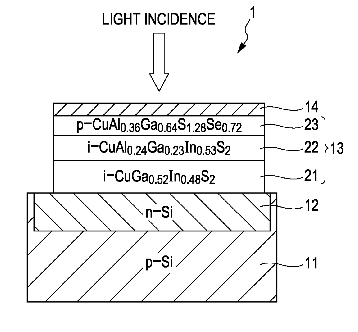
[0074]A first example of a solid-state image device according to a first embodiment of the present invention will be described with reference to a schematic cross-sectional view of FIG. 1.

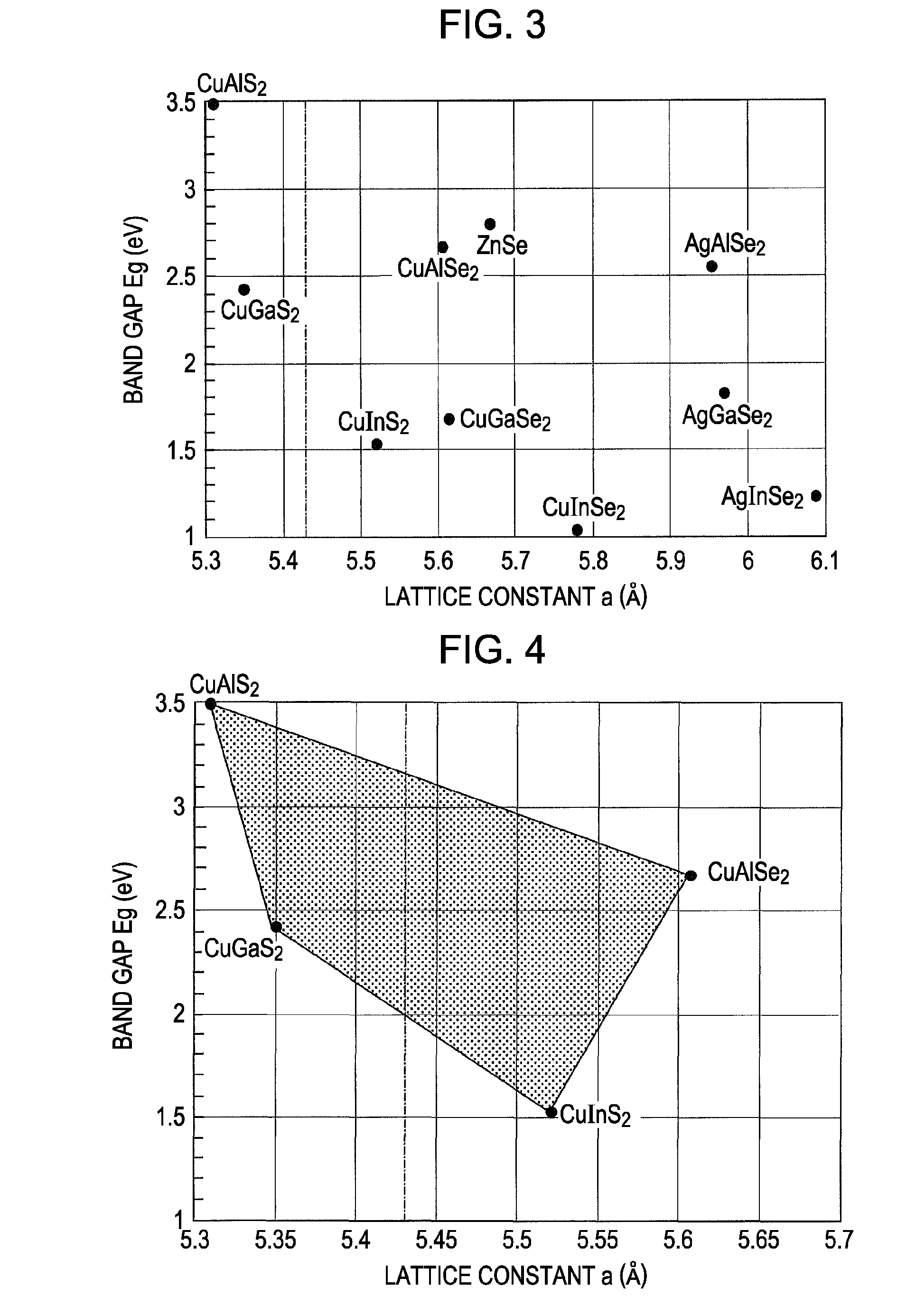
[0075]As shown in FIG. 1, a first electrode layer 12 is formed in a silicon substrate 11. The first electrode layer 12 is made of, for example, an n-type silicon region formed in the silicon substrate 11. A photoelectric conversion layer 13 composed of chalcopyrite-based compound semiconductors of lattice-matched copper-aluminum-gallium-indium-sulfur-selenium (hereinafter, referred to as “CuAlGaInSSe”)-based mixed crystals is arranged on the first electrode layer 12. Copper-aluminum-gallium-indium-zinc-sulfur-selenium (hereinafter, referred to as “CuAlGaInZnSSe”)-based mixed crystals may also be used as the chalcopyrite-based compound semiconductors described above. An optically transparent second electrode layer 14 is arrange...

second embodiment

2. Second Embodiment

Second Example of Structure of Solid-State Image Device

[0101]A second example of a solid-state image device according to a second embodiment of the present invention will be described with reference to a schematic cross-sectional view of FIG. 12, a schematic circuit diagram of FIG. 13, the circuit being configured to read a signal, and FIG. 14 which is a band diagram at zero bias. A structure in which signal readout and avalanche multiplication are allowed to occur simultaneously will be described below.

[0102]As shown in FIGS. 12 and 13, the silicon substrate 11 is a p-type silicon substrate. The first electrode layer 12 is formed in the silicon substrate 11. The first electrode layer 12 is made of, for example, an n-type silicon layer formed in the silicon substrate 11. The photoelectric conversion layer 13 composed of lattice-matched CuAlGaInSSe-based mixed crystals is arranged on the first electrode layer 12. The photoelectric conversion layer 13 includes the ...

third embodiment

3. Third Embodiment

Third Example of Structure of Solid-State Image Device

[0116]The structure that separates light in the depth direction and the structure that simultaneously causes the dispersion of light and avalanche multiplication have been described above. As a third embodiment of the present invention, a simple structure in which only avalanche multiplication occurs can be used. An exemplary structure will be described with reference to FIG. 19 which is a band diagram at zero bias and FIG. 20 which is a band diagram at a reverse bias.

[0117]As shown in FIGS. 19 and 20, a continuous or stepwise change in band gap results in a high degree of discontinuity. In this case, the degree of conduction-band discontinuity is higher than that of the case shown in FIGS. 14 to 17. It is thus possible to achieve a high avalanche multiplication gain at a low driving voltage. In this case, color separation may be performed with a color filter such as an on-chip color filter (OCCF) arranged adja...


PUM


Abstract

A solid-state image device includes a silicon substrate, and a photoelectric conversion layer arranged on the silicon substrate and lattice-matched to the silicon substrate, the photoelectric conversion layer being composed of a chalcopyrite-based compound semiconductor of a copper-aluminum-gallium-indium-sulfur-selenium-based mixed crystal or a copper-aluminum-gallium-indium-zinc-sulfur-selenium-based mixed crystal.

Description

BACKGROUND OF THE INVENTION[0001]1. Field of the Invention[0002]The present invention relates to a solid-state image device, a method for producing the solid-state image device, and an image pickup apparatus.[0003]2. Description of the Related Art[0004]There have been advances in the development of a reduction in pixel size as the number of pixels is increased. Meanwhile, there have also been advances in the development of improvement in motion-picture performance by high-speed imaging. In this way, high-speed imaging and the reduction in pixel size reduce the number of photons incident on one pixel, reducing sensitivity.[0005]For surveillance cameras, there is a demand for cameras capable of capturing images in a dark place. That is, there is a demand for high-sensitivity sensors.[0006]In an image sensor having the typical Bayer pattern, pixels are separated for each color. Thus, demosaicing, which is arithmetic processing to interpolate the color of a pixel from pixels surrounding...

Claims


Application Information

Patent Timeline
Patent Type & Authority Applications(United States)
IPC IPC(8): H04N5/335H04N5/225H01L31/18H01L31/14
CPCH01L27/14645H01L27/14683H01L31/0322H01L31/107H01L31/109H04N9/045Y02E10/541Y02P70/521H01L27/1464Y02P70/50
Inventor TODA, ATSUSHI
Owner SONY CORP
Why Eureka
Try Eureka