Method for Manufacturing Crystalline Semiconductor Film and Method for Manufacturing Thin Film Transistor

a manufacturing method and technology of crystalline semiconductors, applied in the direction of crystal growth process, polycrystalline material growth, chemically reactive gases, etc., can solve the problems of difficult generation of crystal nuclei, large plasma damage to a surface, etc., to achieve large on-current, high carrier mobility, and uniform grain siz

Inactive Publication Date: 2010-08-26
SEMICON ENERGY LAB CO LTD
View PDF19 Cites 25 Cited by
  • Summary
  • Abstract
  • Description
  • Claims
  • Application Information

AI Technical Summary

Benefits of technology

[0021]According to one embodiment of the present invention, a crystalline semiconductor film in which crystal grain sizes are large and uniformity of the grain sizes is high compared to the conventional one can be manufactured while plasma damage to a surface over which the crystalline semiconductor film is to be formed is suppressed. In such a crystalline semiconductor film, carrier mobility is high and on-current is large.
[0022]Further, according to one embodiment of the present invention, a bottom-gate thin film transistor can be manufactured which has fewer defects at an interface between a gate insulating film and a crystalline semiconductor film or / and in the gate insulating film. In particular, by reducing defects at the interface between the gate insulating film and the crystalline semiconductor film, a thin film transistor in which an amount of the threshold voltage shift is small can be manufactured.

Problems solved by technology

However, many grain boundaries exist in a formed microcrystalline semiconductor film because crystal grain sizes are small.
On the other hand, in a condition where a flow ratio of a deposition gas to a dilution gas is low (a condition where a dilution ratio is high), crystal nuclei are difficult to generate (a semiconductor material is difficult to deposit).
Thus, plasma damage to a surface over which a microcrystalline semiconductor film is to be formed is relatively large and the grain sizes are nonuniform.

Method used


Image

  • Method for Manufacturing Crystalline Semiconductor Film and Method for Manufacturing Thin Film Transistor
  • Method for Manufacturing Crystalline Semiconductor Film and Method for Manufacturing Thin Film Transistor
  • Method for Manufacturing Crystalline Semiconductor Film and Method for Manufacturing Thin Film Transistor

Examples


embodiment 1

[0047]In this embodiment, a method for manufacturing a crystalline semiconductor film is described with reference to accompanying drawings. Here, as one example of a crystalline semiconductor film, crystalline silicon is used.

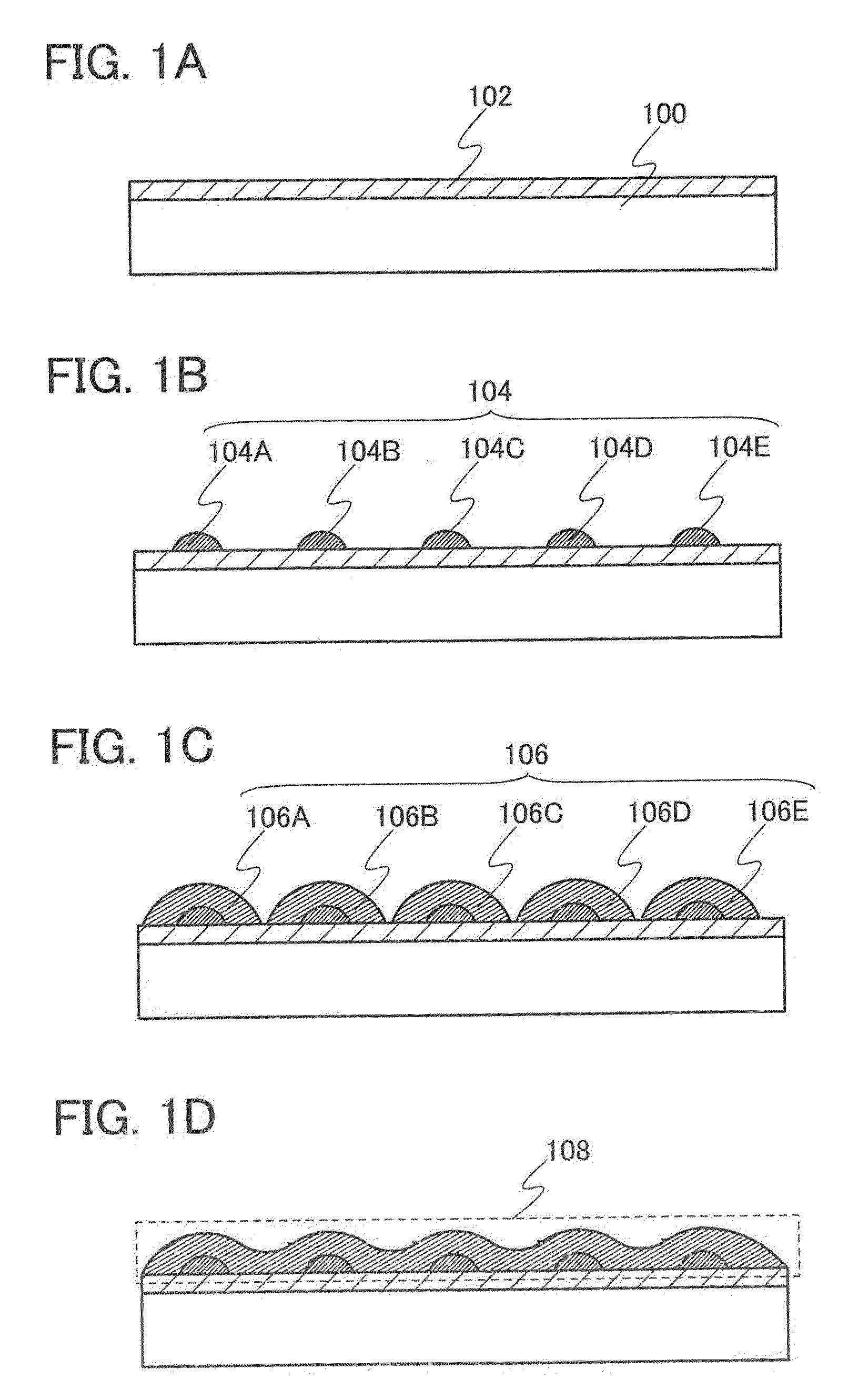
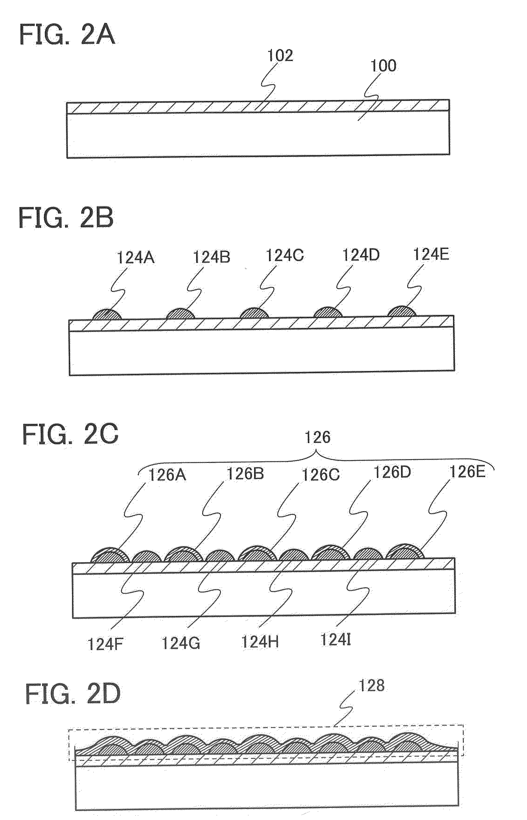
[0048]First, a substrate 100 is prepared. The substrate 100 is not limited to a substrate formed of a particular material as long as the substrate 100 has heat resistance and chemical resistance that can withstand formation of each thin film (e.g., a thin film of crystalline silicon) formed over the substrate 100. As the substrate 100, for example, a glass substrate, a quartz substrate, a stainless steel substrate, and a silicon substrate are given.

[0049]Next, an insulating film 102 is formed over the substrate 100 (see FIG. 1A). Here, the insulating film 102 is preferably a silicon oxide film. Note that the insulating film 102 does not need to be provided in the case where there is no particular necessity for it.

[0050]Next, a crystalline semiconductor film is ...

embodiment 2

[0072]In this embodiment, a method for manufacturing a thin film transistor, to which the method for manufacturing the crystalline semiconductor film described in Embodiment 1 is applied, is described with reference to drawings.

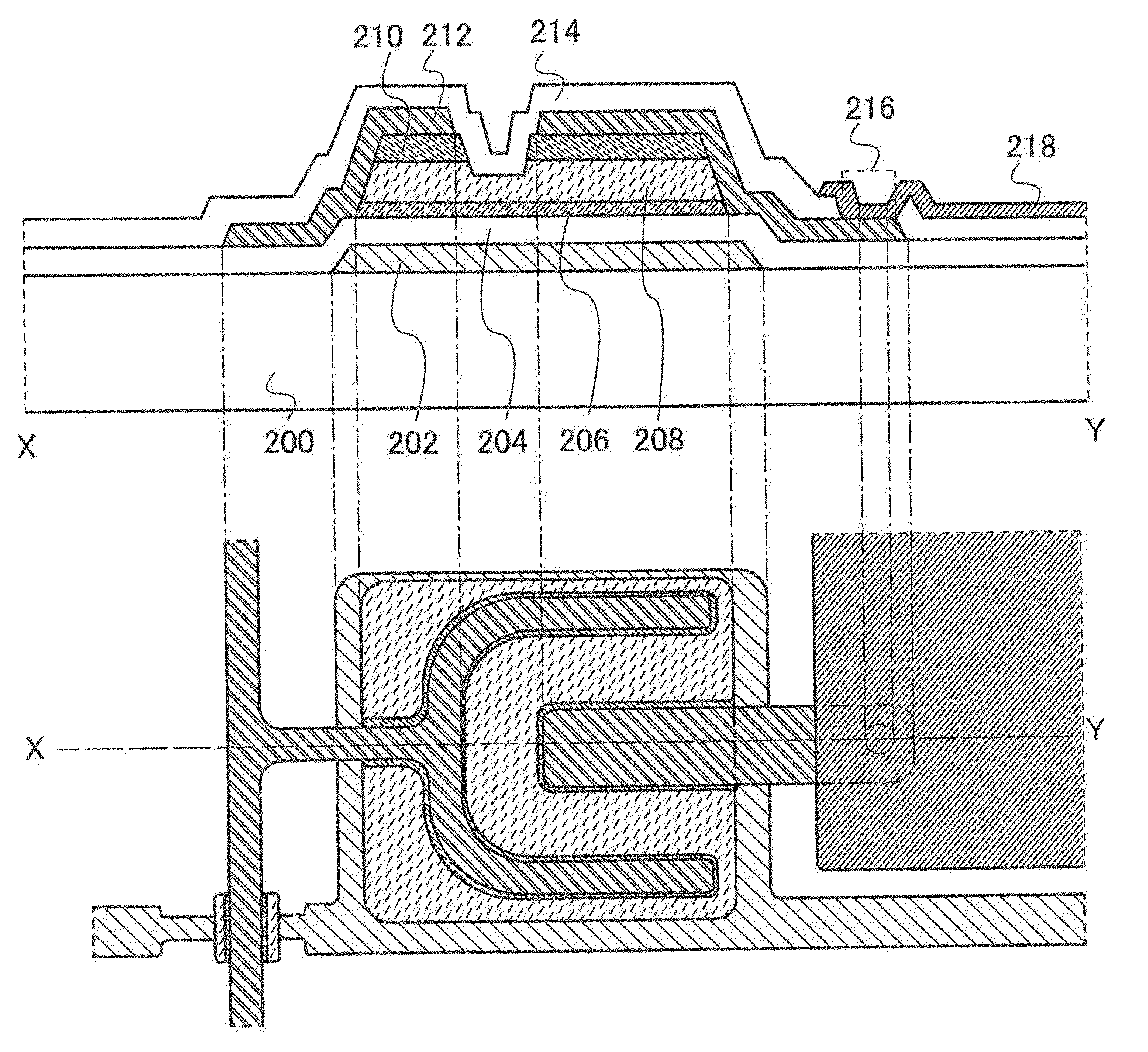
[0073]FIG. 4 illustrates an example of a top view and a cross-sectional view of a thin film transistor of this embodiment. The thin film transistor illustrated in FIG. 4 includes a gate electrode layer 202 over a substrate 200, a gate insulating layer 204 covering the gate electrode layer 202, a crystalline semiconductor layer 206 over the gate insulating layer 204, an amorphous semiconductor layer 208 over the crystalline semiconductor layer 206, a source and a drain regions 210 over part of the amorphous semiconductor layer 208, a source and a drain electrode layers 212 over the source and the drain regions 210, and an insulating layer 214 over the source and the drain electrode layers 212. Each layer is patterned into a desired shape. The amorphous semicon...

embodiment 3

[0148]In this embodiment, a method for manufacturing a thin film transistor, to which the method for manufacturing the crystalline semiconductor film described in Embodiment 1 is applied, and which differs from the method in Embodiment 2 is described with reference to drawings. Specifically, a method for manufacturing a thin film transistor using a multi-tone mask is described.

[0149]Here, a multi-tone mask refers to a mask capable of light exposure with three levels of light intensity to provide an exposed region, a half-exposed region, and an unexposed region. With the use of the multi-tone mask, a resist mask with plural thicknesses (typically, two kinds of thicknesses) can be formed by one-time exposure and development process. Thus, the use of the multi-tone mask can reduce the number of photomasks.

[0150]FIG. 9A-1 and FIG. 9B-1 illustrate cross-sectional views of typical multi-tone masks. FIG. 9A-1 illustrates a gray-tone mask 300 and FIG. 9B-1 illustrates a half-tone mask 305.

[...


PUM

PropertyMeasurementUnit
deposition rateaaaaaaaaaa
pressureaaaaaaaaaa
temperatureaaaaaaaaaa

Abstract

A crystalline semiconductor film is manufactured by a first step in which a crystalline semiconductor film is formed on and in contact with an insulating film and a second step in which the crystalline semiconductor film is grown in a condition where a generation frequency of nuclei is lower than in the first step. The second step is conducted in a condition where a flow ratio of a semiconductor material gas to a deposition gas is lower than in the first step. Thus, a crystalline semiconductor film whose crystal grains are large and uniform can be obtained and plasma damage to a base film of the crystalline semiconductor film can be reduced compared with a crystalline semiconductor film in a conventional method.

Description

BACKGROUND OF THE INVENTION[0001]1. Field of the Invention[0002]The present invention relates to a manufacturing method of a crystalline semiconductor film and a manufacturing method of a thin film transistor. Further, the present invention relates to a semiconductor device such as a display device using them.[0003]2. Description of the Related Art[0004]In recent years, a thin film transistor including a semiconductor thin film (with a thickness of several nanometers to several hundreds nanometers, approximately) over a substrate having an insulating surface (e.g., a glass substrate) has been attracting attention. Thin film transistors are widely used for ICs (integrated circuits) and electronic devices such as electro-optical devices. In particular, thin film transistors are rapidly developed as switching elements of image display devices typified by liquid crystal display devices and the like. In an image display device such as a liquid crystal display device, a thin film transist...

Claims


Application Information

Patent Timeline
Patent Type & Authority Applications(United States)
IPC IPC(8): H01L21/336H01L21/20
CPCH01L21/02532H01L21/02645H01L27/1288H01L29/66765H01L29/04
Inventor YOKOI, TOMOKAZUTAJIMA, RYOTA
Owner SEMICON ENERGY LAB CO LTD
Why Eureka
Try Eureka