
Method of producing epitaxial wafer as well as epitaxial wafer

a technology of epitaxial wafers and epitaxial wafers, which is applied in the direction of non-metal conductors, conductors, and under a protective fluid, can solve the problems of poor gettering ability, poor influence of the region adjacent to the surface of the device on the device properties, and poor deterioration of the gate oxide integrity of the cop

Inactive Publication Date: 2011-03-03
SUMCO CORP
View PDF9 Cites 7 Cited by
  • Summary
  • Abstract
  • Description
  • Claims
  • Application Information

AI Technical Summary

Benefits of technology

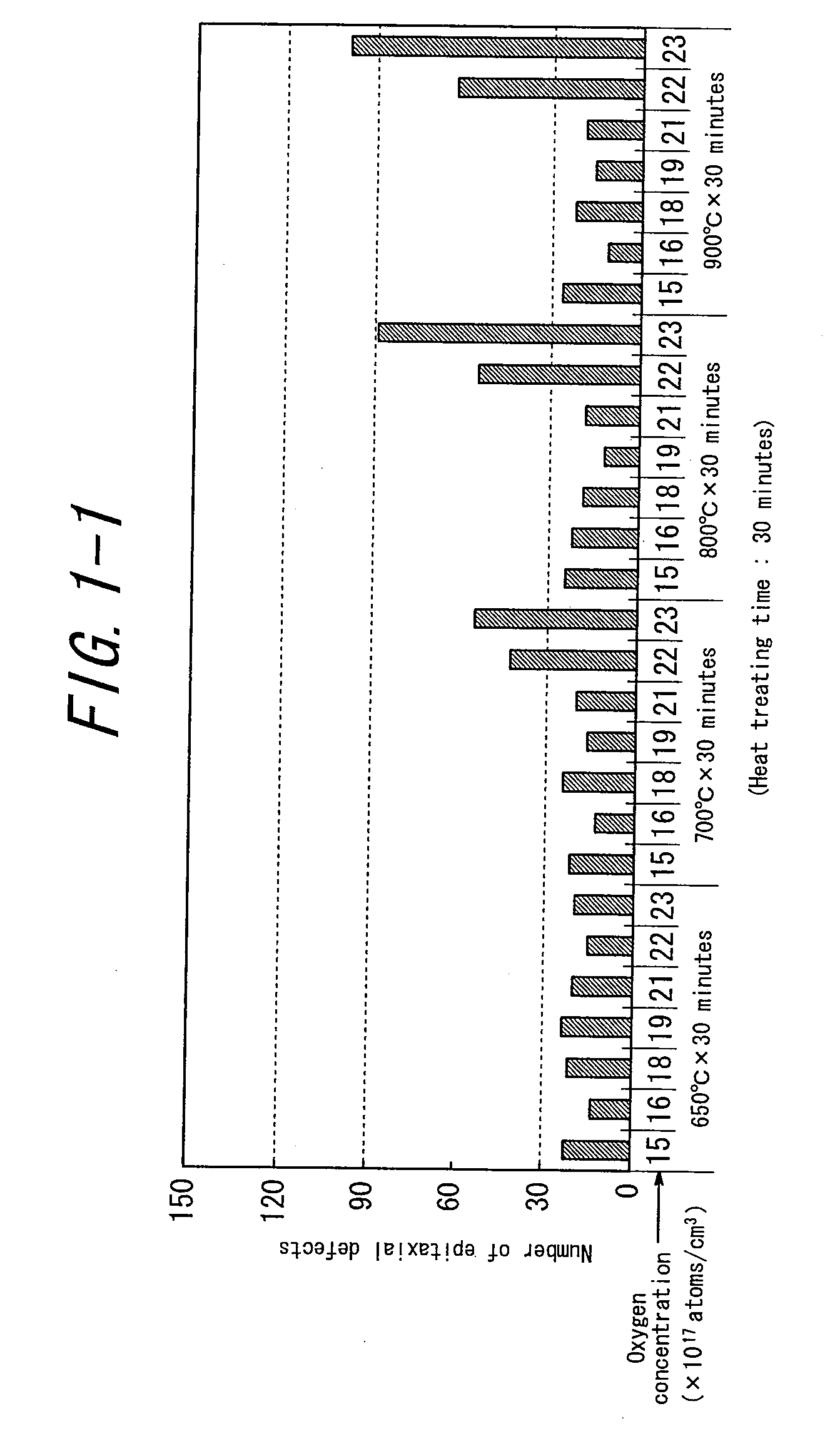
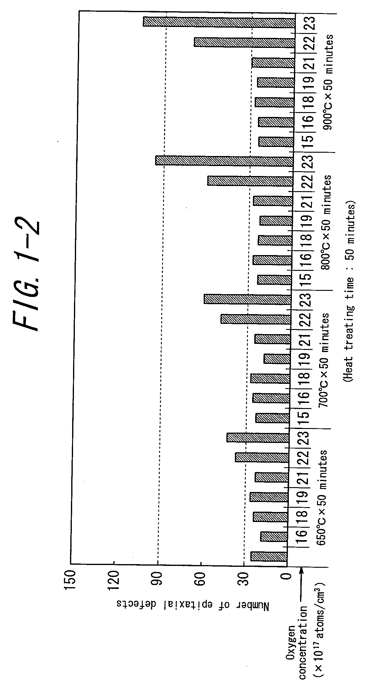
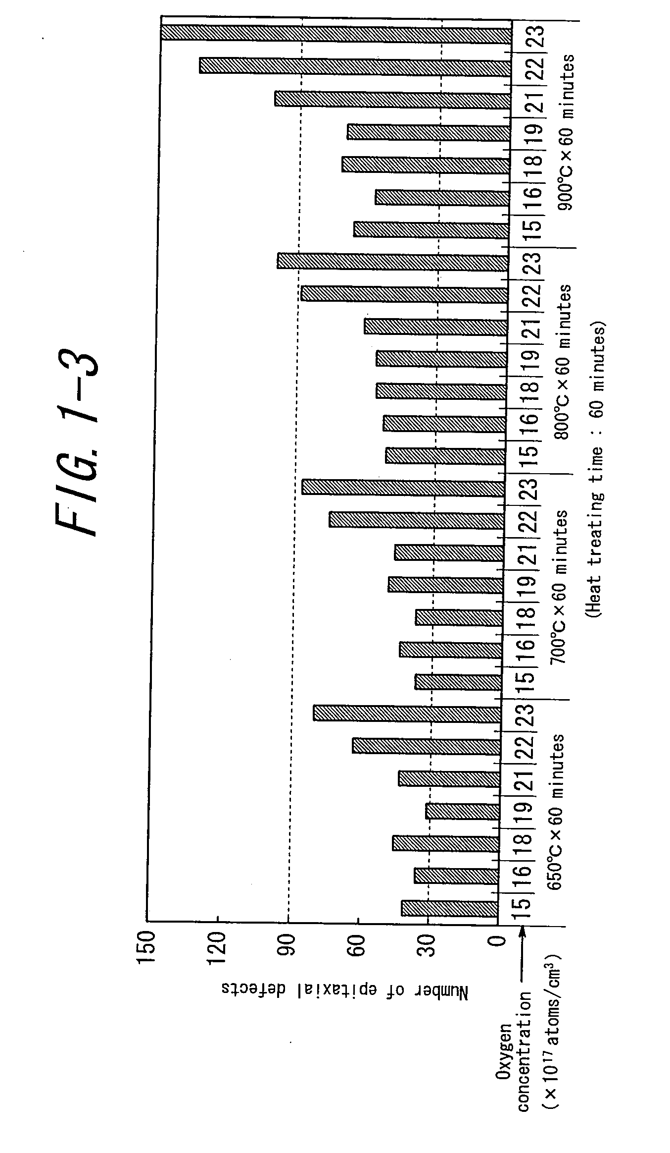
[0017]In order to solve the above problems, the inventors have made various studies without sticking to the common belief that epitaxial defects occur as the oxygen concentration in the wafer becomes too high and investigated production conditions causing no disadvantage even when it is first essential to increase the oxygen concentration in the wafer, and as a result, there is obtained a new knowledge that, as long as a heat treatment is conducted under certain pre-annealing conditions before epitaxial growth, even when using a wafer with excessively increased oxygen concentration, it is possible to obtain an epitaxial wafer causing no epitaxial defect and being excellent in the gettering ability and low in the occurrence of thermal donor.
[0029]Therefore, the epitaxial wafer obtained according to the method of the invention has an oxygen precipitation nuclei of not less than 1×10⁹ / cm3 within a depth of 10 μm just beneath the epitaxial layer, which has not been seen in the conventional wafer, and is excellent in the gettering ability.

Problems solved by technology

It is known that the COP deteriorates a gate oxide integrity since it accelerates thinning of the gate oxide film.
However, the precipitation of oxygen in the active region adjacent to the surface of the device exerts a bad influence on device properties.
Thus, sufficient oxygen precipitation is not caused in the recent device process with a lower temperature, so that the gettering ability is lacking, and in many cases the metal contamination of the active layer in the device cannot be prevented effectively.
On the other hand, when oxygen precipitates are existent on the surface portion of the wafer in the production of epitaxial wafers, there is a problem that stacking faults (epitaxial defects) are caused in the resulting epitaxial layer due to oxygen precipitates on the surface portion and the latter half of the crystal cannot be used, lowering the yield.
In the above pre-annealing method, the oxygen concentration is low, which can reduce the occurrence of epitaxial defects due to oxygen precipitates, but the proximity gettering effect is low and an epitaxial wafer having sufficient oxygen precipitates cannot be produced.
In the above nitrogen-doping method, an epitaxial wafer having an oxygen precipitate density to some extent can be obtained, but there is a problem that epitaxial defects due to nitrogen or oxygen precipitates easily occur.
Moreover, there is a problem that the scattering of the oxygen precipitate density is caused in a length direction of the single crystal ingot due to the segregation of nitrogen concentration.
However, there is caused a disadvantage that the resistivity is changed by the oxygen donor.

Method used


Image

  • Method of producing epitaxial wafer as well as epitaxial wafer
  • Method of producing epitaxial wafer as well as epitaxial wafer
  • Method of producing epitaxial wafer as well as epitaxial wafer

Examples


Embodiment Construction

[0039]The experimental results leading to the invention will be described in detail below.

[0040]First, it is necessary to increase an oxygen concentration itself of a wafer to be epitaxially grown up to a higher level exceeding the conventional common wisdom in order to provide an epitaxial wafer having a high gettering ability demanded particularly recently. Based on this, the inventors have made various studies on conditions enabling to use a wafer with a high oxygen concentration as follows.

[0041]The oxygen concentration in a silicon single crystal is determined by three factors of (1) melting of quartz into a silicon melt, (2) transferring of a melt and (3) evaporation from a melt surface.

[0042]In the experiments of the invention, quartz rings with different sizes are placed on a bottom of a quartz crucible, and polycrystalline silicon materials are filled thereon and then melted under heating. By placing the quartz rings in the quartz crucible is increased a contact area betwee...


PUM

PropertyMeasurementUnit
temperatureaaaaaaaaaa

Abstract

An epitaxial wafer is produced by a method comprising steps of growing a silicon single crystal ingot having a given oxygen concentration through Czochralski method, cutting out a wafer from the silicon single crystal ingot, subjecting the wafer to a heat treatment at a given temperature for a given time, and epitaxially growing the wafer.

Description

BACKGROUND OF THE INVENTION[0001]1. Field of the Invention[0002]This invention relates to a method of producing a silicon single crystal wafer, and more especially to a method of producing a silicon single crystal wafer grown through Czochralski method (CZ method) and preferably used as a substrate for a semiconductor device. Moreover, this invention relates to an epitaxial wafer having high-density oxygen precipitation nuclei just beneath an epitaxial layer and being preferably used as a substrate for a semiconductor device.[0003]2. Description of the Related Art[0004]The silicon single crystal grown through the CZ method includes void defects generally referred to as COP (crystal originated particles). It is known that the COP deteriorates a gate oxide integrity since it accelerates thinning of the gate oxide film.[0005]Also, since supersaturated oxygen is soluted in the silicon single crystal grown through the CZ method, the supersaturated oxygen is precipitated as SiO2 in a devi...

Claims


Application Information

Patent Timeline
Patent Type & Authority Applications(United States)
IPC IPC(8): H01B1/04C30B15/00B32B9/00
CPCC30B15/00C30B25/186H01L21/3225C30B29/06C30B25/20
Inventor UMENO, SHIGERUONO, TOSHIAKISUGIMURA, WATARU
Owner SUMCO CORP
Learn More