Method for manufacturing nitrogen compound semiconductor substrate and nitrogen compound semiconductor substrate, and method for manufacturing single crystal sic substrate and single crystal sic substrate

Active Publication Date: 2011-04-21
AIR WATER INC
View PDF2 Cites 5 Cited by
  • Summary
  • Abstract
  • Description
  • Claims
  • Application Information

AI Technical Summary

Benefits of technology

[0030]That is, in the method for manufacturing the nitrogen compound semiconductor substrate according to the aspect of the invention, when converting the surface Si layer into the single crystal SiC layer, by leaving the surface Si layer in the vicinity of the interface with the embedded insulating layer as the residual Si layer, the flatness of the interface of the residual Si layer and the embedded insulating layer below the residual Si layer can dramatically be improved, and the “waviness” in the interface can dramatically be decreased. Thus, because the flatness of the interface of the embedded insulating layer and the residual Si layer improves, the “waviness” which occurs in the single crystal SiC layer itself formed on the surface can dramatically be suppressed. Thus, because the single crystal SiC layer with less waviness is formed, the nitrogen compound semiconductor formed on the single crystal SiC layer by the epitaxial growth can also be dramatically improved in crystallinity, and a performance as a semiconductor device can dramatically be improved. Moreover, because it does not depend on an ion implantation or the like, the nitrogen compound semiconductor substrate as the high quality semiconductor device described above can be manufactured with low cost and high productivity.
[0031]In the aspect of the invention, if epitaxially growing the single crystal SiC further on the denatured single crystal SiC layer and epitaxially growing the nitrogen compound semiconductor on the epitaxially-grown single crystal SiC, because the crystallinity of the growing SiC improves when further forming SiC as an upper layer of the single crystal SiC layer by the epitaxial growth, the crystallinity of the nitrogen compound semiconductor epitaxially grown on SiC becomes high, and, thereby, a good nitrogen compound semiconductor device can be obtained.
[0032]In the aspect of the invention, if the thickness of the residual Si layer is 3 to 20 nm, an effect for improving the flatness of the interface of the embedded insulating layer and the residual Si layer, and the single crystal SiC layer itself can sufficiently be obtained, and defects such as voids are hardly caused in the lower layers of the single crystal SiC layer. Therefore, a good nitrogen compound semiconductor device can be obtained.
[0033]In the nitrogen compound semiconductor substrate of the aspect of the invention, when converting the surface Si layer into the single crystal SiC layer, by leaving the Si layer in the vicinity of the interface with the embedded insulating layer as the residual. Si layer, the flatness of the interface of t

Problems solved by technology

However, in the above method where the silicon carbide layer is epitaxially grown on the SOI substrate and the nitride semiconductor layer is further epitaxially grown on the silicon carbide layer, there has been a problem in which crystal defects easily occur in an interface of the silicon carbide and the silicon.
However, by doing this, an irregular and large “waviness” occurs in an interface of the embedded oxide film and the SiC thin film.
That is, because the interface of the converted SiC layer and the embedded SiO2 layer is unstable under the high temperature and, especially, the Si→SiC reaction rapidly progresses in addition to SiC tends to enter the SiO2

Method used


Image

  • Method for manufacturing nitrogen compound semiconductor substrate and nitrogen compound semiconductor substrate, and method for manufacturing single crystal sic substrate and single crystal sic substrate
  • Method for manufacturing nitrogen compound semiconductor substrate and nitrogen compound semiconductor substrate, and method for manufacturing single crystal sic substrate and single crystal sic substrate
  • Method for manufacturing nitrogen compound semiconductor substrate and nitrogen compound semiconductor substrate, and method for manufacturing single crystal sic substrate and single crystal sic substrate

Examples


example a

EXAMPLE A1

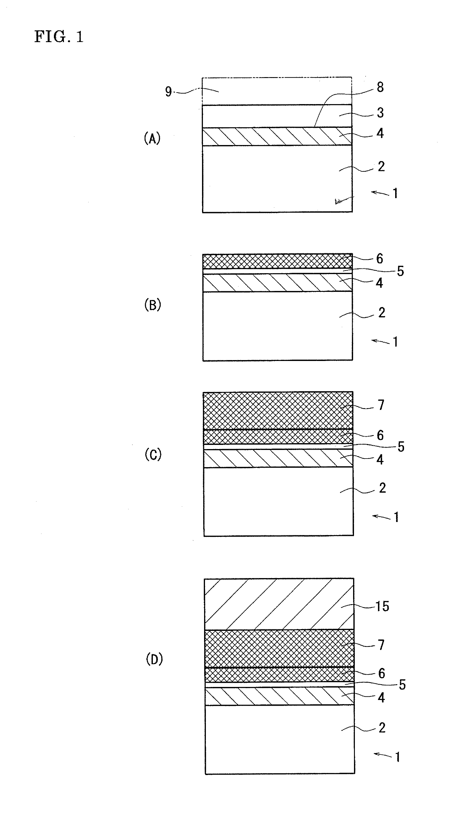
[0096]A (111) SIMOX substrate of which the thickness of the surface Si layer 3 therein is 10 to 14 nm (SOI-A), a (111) SIMOX substrate of which the thickness of the surface Si layer 3 therein is 18 to 22 nm (SOI-B), and a (111) SOI substrate of such attachment (SOI-C) are prepared as starting materials. Each SOI substrate is inserted into an electric furnace as a specimen, and propane and hydrogen gas are introduced into the electric furnace at flow rates of 100 seem and 10 SLM respectively so that an atmosphere in the electric furnace is heated to reach a temperature of 1250° C., then kept for 15 minutes at the same temperature.

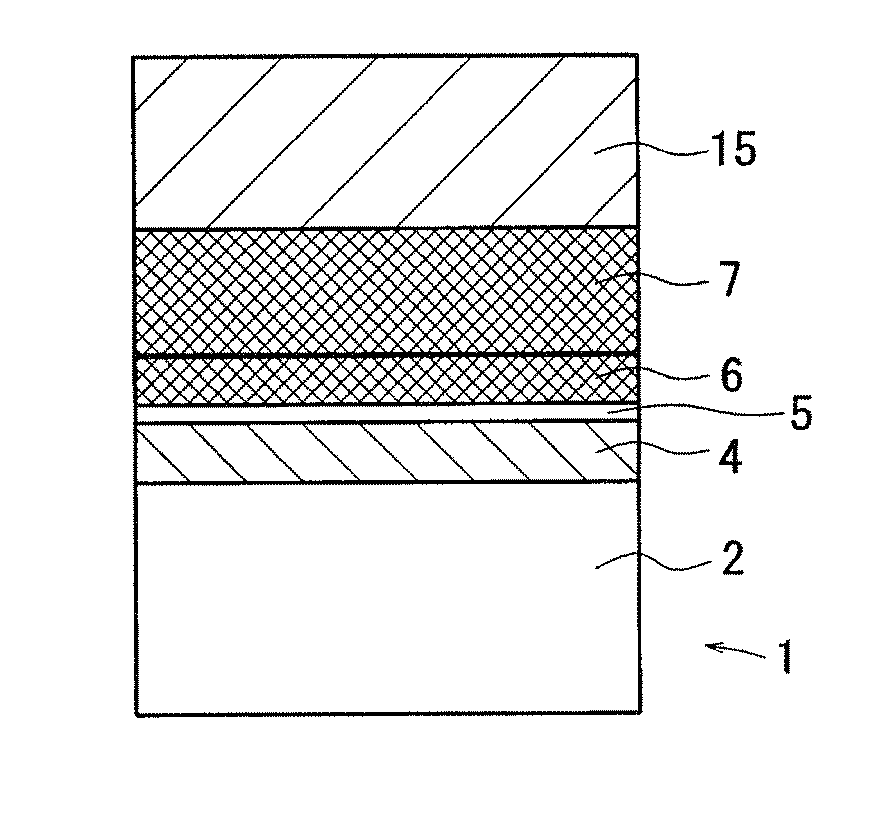
[0097]By this step, a silicon layer of 3 to 7 nm from the surface side of each surface Si layer 3 is carbonized to convert it into the single crystal SiC layer 6 of 3 to 7 nm thickness (seed layer). Thereby, SOI-A, SOI-B, and SOI-C have a film structure in which the residual Si layers 5 of 3 to 11 nm, 9 to 19 nm, and approximately 9900 to 1100 nm r...

example a2

[0102]A (111) SIMOX substrate of which the thickness of the surface Si layer 3 therein is 10 to 14 nm (SOI-A), a (111) SIMOX substrate of which the thickness of the surface Si layer 3 therein is 18 to 22 nm (SOI-B), and a (111) SOI substrate of such attachment (SOI-C) are prepared as starting materials, to and are operated a carbonization and heat treatment under the same condition with the Example Al. By this step, a silicon layer of 3 to 7 nm from the surface side of each surface Si layer 3 is carbonized to convert it into the single crystal SiC layer 6 of 3 to 7 nm thickness. Thereby, SOI-A, SOI-B, and SOI-C have a film structure in which the residual Si layers 5 of 3 to 11 nm, 9 to 19 nm, and approximately 9900 to 1100 nm remains in the lower layer parts thereof, respectively.

[0103]Continuously, the wafer is inserted into the depressurized epitaxial-growth furnace and heated so that the temperature of the wafer reaches 1150° C. while 3 seem of monomethylsilane is introduced into...

example b

[0147]Next, descriptions will be given about an Example B of the method of the single crystal SiC substrate in the present invention.


PUM

PropertyMeasurementUnit
Thicknessaaaaaaaaaa
Nanoscale particle sizeaaaaaaaaaa

Abstract

In order to provide a method for manufacturing a single crystal SiC substrate that can obtain an SiC layer with good crystallinity, an Si substrate 1 having a surface Si layer 3 of a predetermined thickness and an embedded insulating layer 4 is prepared, and when the Si substrate 1 is heated in a carbon-series gas atmosphere to convert the surface Si layer 3 into a single crystal SiC layer 6, surface Si layer 3 into a single crystal SIC layer 6, the Si layer in the vicinity of an interface 8 with the embedded insulating layer 4 is left as a residual Si layer 5.

Description

TECHNICAL FIELD[0001]The present invention relates to a method for manufacturing a nitrogen compound semiconductor substrate as a semiconductor substrate of an insulating-layer-embedded type and the nitrogen compound semiconductor substrate manufactured by the method, and a method for manufacturing a single crystal SiC substrate as a semiconductor substrate of the insulating-layer-embedded type and the single crystal SiC substrate manufactured by the method.RELATED ART[0002]A nitrogen compound, such as gallium nitride and aluminum nitride, is a wide gap semiconductor of direct band-gap type, and because it excels, comparing with a silicon semiconductor, in insulation breakdown electric field, saturation electron velocity, and chemical stability, the nitrogen compound has attracted an attention as a material for light-emitting device and semiconductor device for the next generation. An SOI substrate having an embedded insulating layer excels in speed-up and low power consumption of a...

Claims


Application Information

Patent Timeline
IPC IPC(8): H01L29/24C30B25/02C30B25/10C30B29/06C30B29/36
CPCC30B25/02H01L21/8258C30B29/403H01L21/02381H01L21/0254H01L21/8213H01L21/02614C30B29/36H01L21/02447
Inventor KAWAMURA, KEISUKEIZUMI, KATSUTOSHIASAMURA, HIDETOSHIYOKOYAMA, TAKASHI
Owner AIR WATER INC
Why Eureka
Try Eureka