Insulating film for semiconductor device, process and apparatus for producing insulating film for semiconductor device, semiconductor device, and process for producing the semiconductor device

a technology of insulating film and semiconductor device, which is applied in the direction of semiconductor/solid-state device details, coatings, chemical vapor deposition coatings, etc., can solve the problems of reducing the permittivity the loss of the capacity of the insulating layer between the wiring, and the need to reduce the capacity between the wiring, etc., to achieve low carbon content, low leakage current, and low permittivity

Inactive Publication Date: 2011-11-03
MITSUBISHI HEAVY IND LTD +1
View PDF2 Cites 6 Cited by
  • Summary
  • Abstract
  • Description
  • Claims
  • Application Information

AI Technical Summary

Benefits of technology

[0076]The present invention makes it possible to obtain an insulating film for a semiconductor device which has characteristics of a low carbon content, a low permittivity, a low leakage current, and a high mechanical strength, and which undergo...

Problems solved by technology

For the increase in the degree of integration and speed-up of the LSIs, miniaturization thereof is underway; however, along with the miniaturization, loss due to the capacity of an insulating layer between wirings has become a problem, and reducing the permittivity of the insulating layer has become necessary.
However, when an interlayer insulating film is formed of SiOF, the permittivity of the interlayer insulating film is lower than that of conventional ones; however, since the permittivity thereof is about 3.2 to 3.5, reduction of the capacity between wirings, prevention of delay of signals propagation through wiring, and so on have not been sufficiently achieved.
Meanwhile, when an interlayer insulating film is formed of an organic compound material, a permittivity of 2.7 has been achieved by the film in which fluorine atoms are introduced to polyimide or by aryl ether-based polymers; however, it is not sufficient yet.
A permittivity of 2.4 can be achieved by a vapor-deposited film of parylene; however, since obtained heat resistance is at most about 200 to 300° C., this restricts the manufacturing processes of semiconductor elements.
Meanwhile, the values of 2.0 to 2.5 have been reported as the permittivit...

Method used


Image

  • Insulating film for semiconductor device, process and apparatus for producing insulating film for semiconductor device, semiconductor device, and process for producing the semiconductor device
  • Insulating film for semiconductor device, process and apparatus for producing insulating film for semiconductor device, semiconductor device, and process for producing the semiconductor device
  • Insulating film for semiconductor device, process and apparatus for producing insulating film for semiconductor device, semiconductor device, and process for producing the semiconductor device

Examples


first embodiment

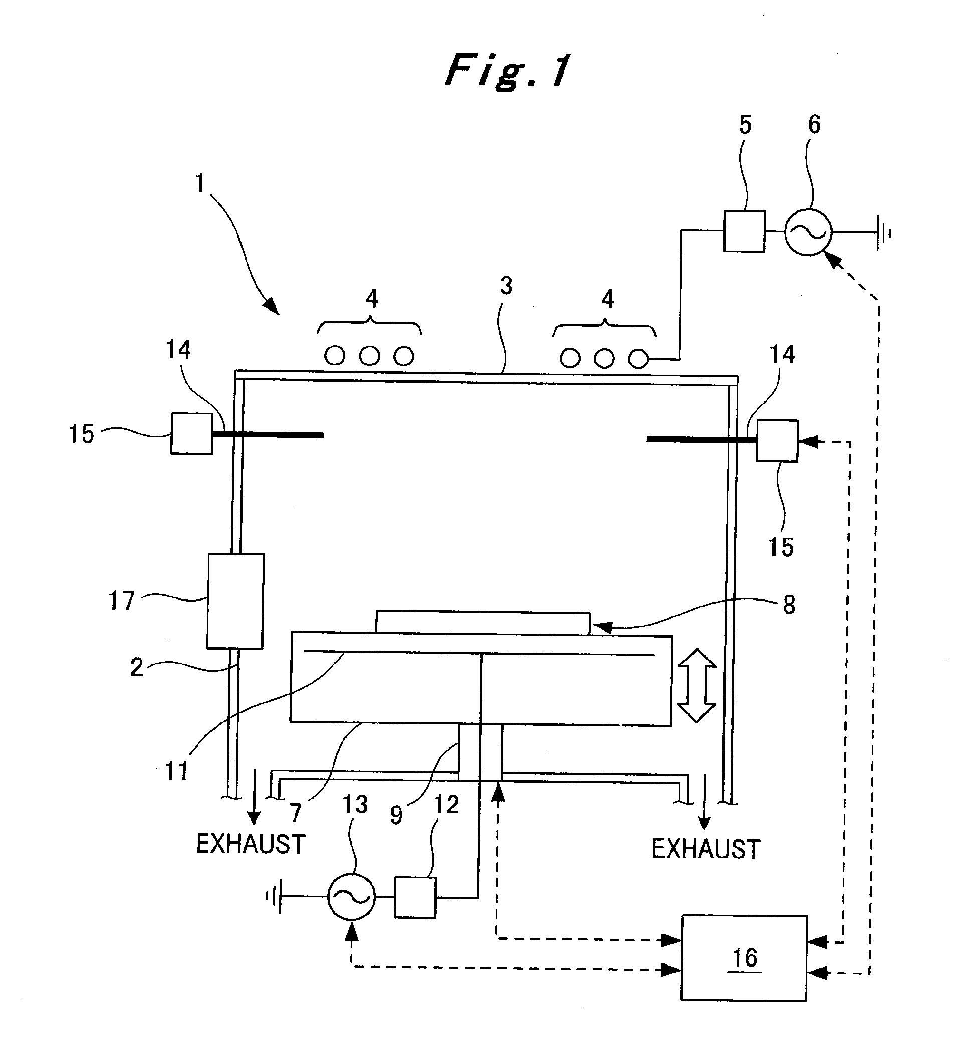
[0103]FIG. 1 is a transparent side view for describing an apparatus for producing an insulating film for a semiconductor device according to the present invention.

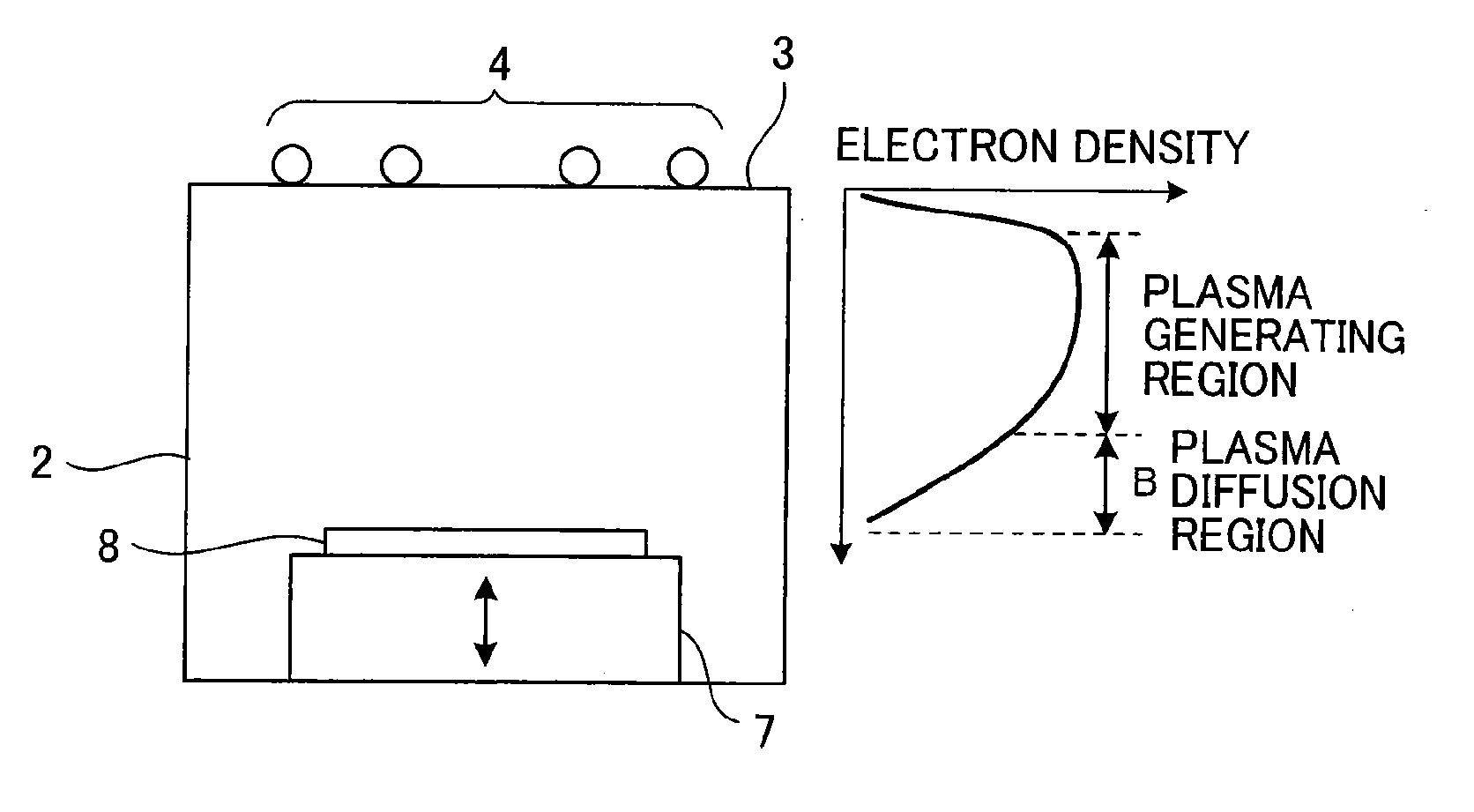
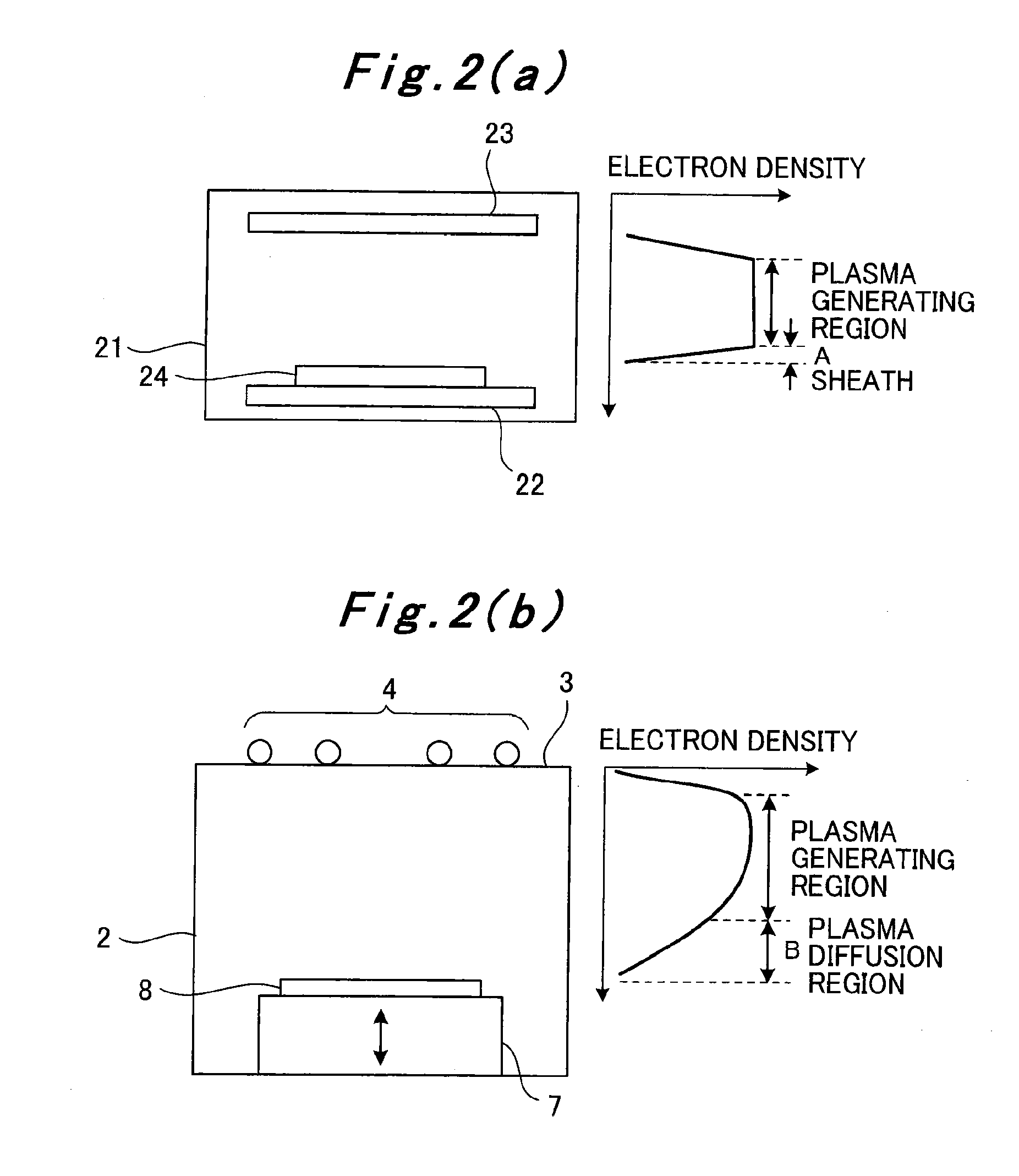
[0104]The plasma CVD apparatus 1 for the insulating film for a semiconductor device according to the present invention has a structure in which the inside of a cylindrical vacuum chamber 2 is used as a film forming chamber. In an upper opening portion of the vacuum chamber 2, a ceramic disk-shaped ceiling plate 3 is disposed to cover the opening portion.

[0105]In addition, a high-frequency antenna 4 formed of, for example, multiple circular rings is placed above (immediately above) the ceiling plate 3. To the high-frequency antenna 4, a high-frequency power source 6 is connected via a matching box 5 (plasma generating means). The high-frequency power source 6 can supply power to the high-frequency antenna 4 at an oscillation frequency (for example, 13.56 MHz) higher than that of a low-frequency power source 13 to be describ...

second embodiment

[0136]A process for producing an insulating film for a semiconductor device of this embodiment is performed on the basis of the production apparatus and the production process described in the first embodiment. Accordingly, in the following, this embodiment is described while description overlapping with that in the first embodiment is omitted.

[0137]In the process for producing an insulating film for a semiconductor device of this embodiment, at least one selected from the group consisting of ammonia and amine compounds each having an alkyl group having 1 to 3 carbon atoms is supplied into the vacuum chamber 2 through the gas nozzles 14, in addition to the mixture gas described in the first embodiment (the carrier gas+the raw material gas obtained by gasifying the alkylborazine compound represented by chemical formula 3). Note that the supply method is not shown in the drawings, but the gases may be supplied by using respective nozzles. Then, electromagnetic waves are radiated into ...

third embodiment

[0143]A process for producing an insulating film for a semiconductor device of this embodiment is also performed on the basis of the production apparatus and the production process described in the first embodiment. Accordingly, in the following, this embodiment is described while description overlapping with that in the first embodiment is omitted.

[0144]The mechanical strength of a borazine skeletal structure film generally needs to be 10 GPa or more in terms of Young's modulus. In this respect, this requirement was met as shown in the graph in FIG. 5(b) to be described below even when no LF power (bias) was applied during the formation of the borazine skeletal structure film (see the Young's modulus at a LF power=0 in the graph in the FIG. 5(b)). However, to further increase the mechanical strength of the borazine skeletal structure film, a LF power is desirably applied to the substrate 8 during film formation by using the low-frequency power source 13. The application of a LF pow...


PUM

PropertyMeasurementUnit
Temperatureaaaaaaaaaa
Fractionaaaaaaaaaa

Abstract

An object is to provide an insulating film for a semiconductor device which has characteristics of a low permittivity, a low leakage current, and a high mechanical strength, undergoes less change in these characteristics with the elapse of time, and has an excellent water resistance, as well as to provide a process and an apparatus for producing the insulating film for a semiconductor device, a semiconductor device, and a process for producing the semiconductor device. A gas containing a raw material gas which gasified a predetermined alkylborazine compound is supplied in a chamber (2); an electromagnetic wave is introduced into the chamber (2) using with an inductive coupling type plasma generation mechanism (4, 5, 6) to convert the gas into a plasma; a substrate (8) is placed in a plasma diffusion region of the plasma; gas-phase polymerization is performed with borazine skeletal molecules, as a fundamental unit, dissociated from the alkylborazine compound by the plasma so as to form the insulating film for semiconductor devices on the substrate (8).

Description

TECHNICAL FIELD[0001]The present invention relates to an insulating film for a semiconductor device for use as an interlayer insulating film, an copper diffusion preventing film, an etch stopper layer, a passivation film, a hard mask, a high-stress film, or the like; a process and an apparatus for producing the insulating film for a semiconductor device; a semiconductor device using the insulating film for a semiconductor device; and a process for producing the semiconductor device.BACKGROUND ART[0002]Recently, along with development of information communication societies, the amount of information processing has been increased, and increase in the degree of integration and speed-up of LSIs (Large Scale Integrated circuits) which carry out the signal processing have been required. For the increase in the degree of integration and speed-up of the LSIs, miniaturization thereof is underway; however, along with the miniaturization, loss due to the capacity of an insulating layer between...

Claims


Application Information

Patent Timeline
IPC IPC(8): H01L21/31C23C16/52C23C16/50H01L21/768H01L23/28
CPCC23C16/342C23C16/507H01L21/02112H01L21/02274H01L21/318H01L2924/0002H01L23/5329H01L2924/00
Inventor KAFUKU, HIDETAKAFUJIWARA, TOSHIHITONISHIMORI, TOSHIHIKOSHIMAZU, TADASHIYASUDA, NAOKINOBUTOKI, HIDEHARUKUMADA, TERUHIKOKAMIYAMA, TAKUYAYAMAMOTO, TETSUYASHIBATA, SHINYA
Owner MITSUBISHI HEAVY IND LTD
Why Eureka
Try Eureka