Method for manufacturing negative electrode active material for non-aqueous electrolyte secondary battery, negative electrode active material for non-aqueous electrolyte secondary battery, negative electrode material for non-aqueous electrolyte secondary battery, negative electrode for non-aqueous electrolyte secondary battery, and non-aqueous electrolyte secondary battery
a technology of non-aqueous electrolyte and active material, which is applied in the direction of final product manufacturing, sustainable manufacturing/processing, cell components, etc., can solve the problems of low efficiency, low level, and inability to fully exploit the potential battery capacity of silicon, etc., to achieve suppressed capacity reduction, small deformation of the effect of battery capacity
- Summary
- Abstract
- Description
- Claims
- Application Information
AI Technical Summary
Benefits of technology
Problems solved by technology
Method used
Image
Examples
example 1
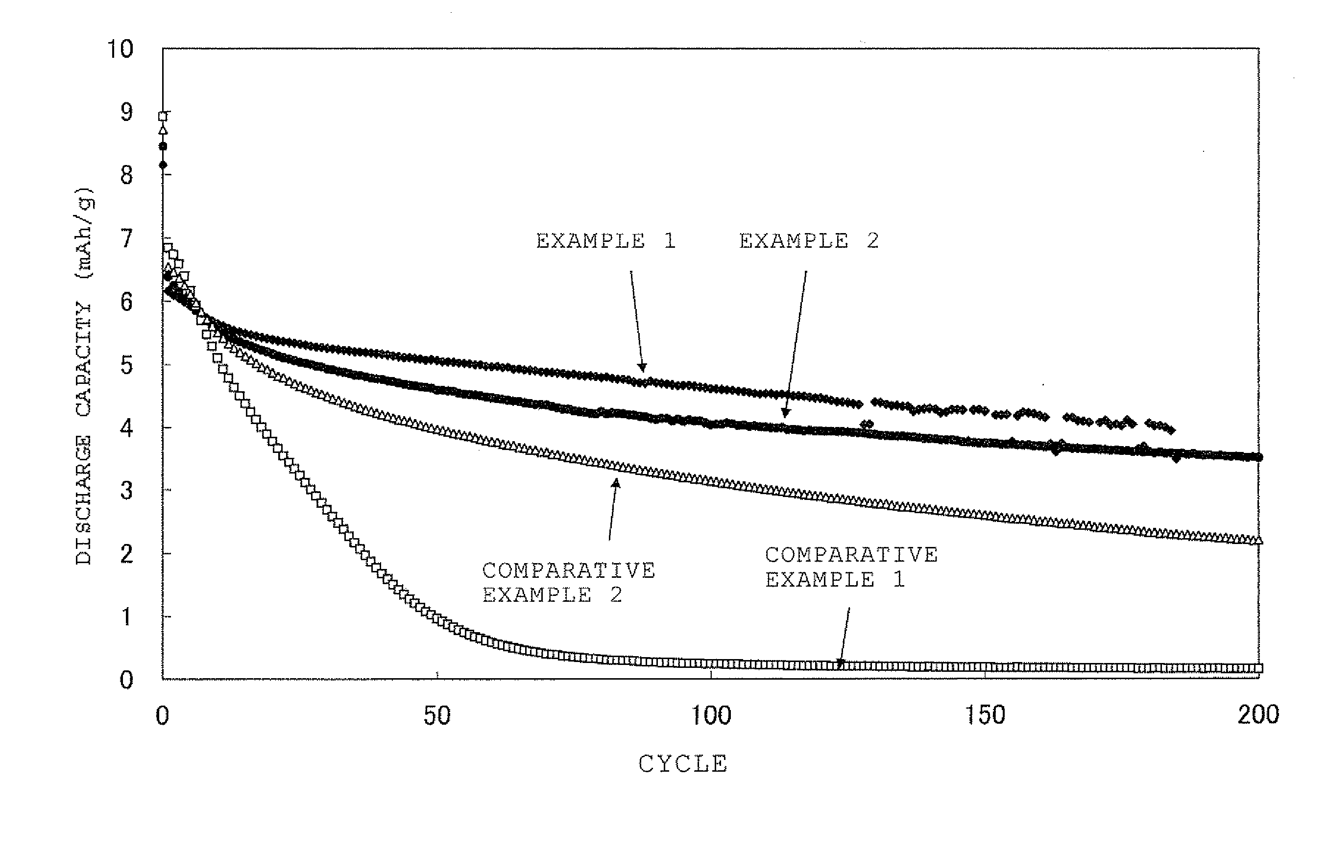
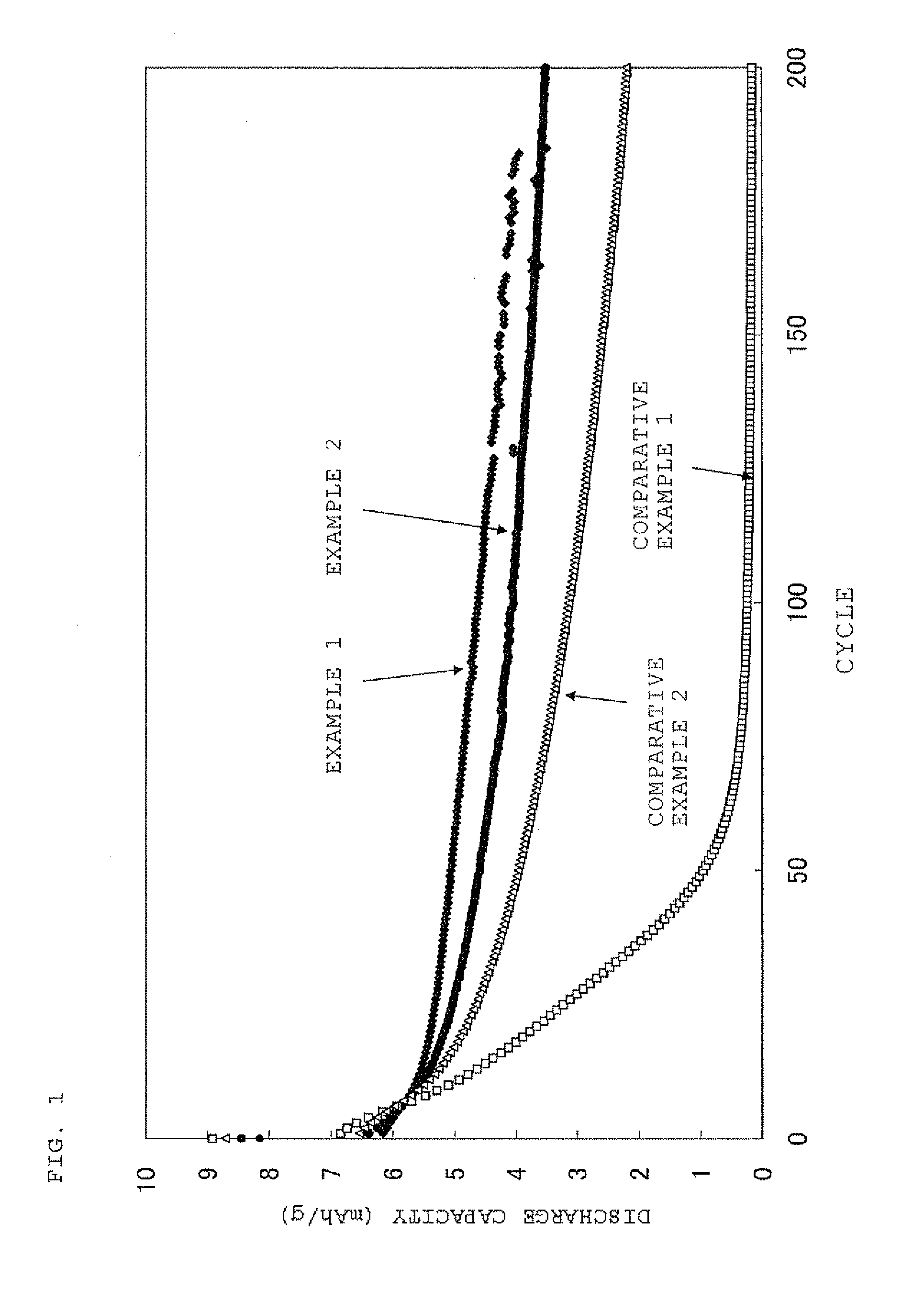
[0153]A copper crucible was installed at the inside of a vacuum chamber having exhaust equipment constituted of an oil diffusion pump, a mechanical booster pump, and an oil-sealed rotary vacuum pump. A metallic silicon bulk of 5 kg was introduced into the copper crucible. The pressure of the chamber was reduced, and the pressure reached 2×10⁻⁴ Pa after 2 hours.
[0154]Next, the metallic silicon bulk was melted by an axial electron gun installed at the bottom of the chamber. After the metallic silicon bulk was melted, vapor deposition process was performed at an output of 150 kW for 1 hour. During the vapor deposition process, the temperature of the vapor deposition substrate made of stainless steel was controlled so as to be 400° C.
[0155]A vapor-deposited silicon of 800 g was obtained after opening the chamber.
[0156]The obtained vapor-deposited silicon was pulverizing at 7,200 rpm with a jet mill (AFG-100 made by Hosokawa Micron Corp.), and thereafter classified by classifier (TC-15 m...
example 2
[0158]Polycrystalline silicon particles were obtained by the same method as Example 1 except that diborane was introduced into the chamber during melting the metallic silicon bulk.
[0159]The polycrystalline silicon particle included boron of 10 ppm (on the basis of mass of the polycrystalline silicon particle after doping) with D50=9.6 μm. It was confirmed that the crystallite size was 45 nm, by the Scherrer method based on the full width at half maximum of the x-ray diffraction line. The true density was 2.309 g / cm3, the compressive strength was 520 MPa, and the BET specific surface area was 0.95 m2 / g.
example 3
[0160]Polycrystalline silicon particles were obtained by the same method as Example 1 except for a temperature of 300° C. of the substrate on which the metallic silicon raw material was vapor-deposited.
[0161]The polycrystalline silicon particle had D50=10.0 μm. It was confirmed that the crystallite size was 20 nm, by the Scherrer method based on the full width at half maximum of the x-ray diffraction line. The true density was 2.290 g / cm3, the compressive strength was 420 MPa, and the BET specific surface area was 1.8 m2 / g.
PUM
| Property | Measurement | Unit |
|---|---|---|
| temperature | aaaaa | aaaaa |
| particle size distribution | aaaaa | aaaaa |
| particle size distribution | aaaaa | aaaaa |
Abstract
Description
Claims
Application Information

