
CMOS moems sensor device

a sensor device and moem technology, applied in the direction of converting sensor output, volume/mass flow by dynamic fluid flow effect, instruments, etc., can solve the problems of low photon emission efficiency, direct band gap semiconductor material, and silicon as poor source of electroluminescent radiation

Inactive Publication Date: 2012-06-21
TSHWANE UNIV OF TECH
View PDF3 Cites 7 Cited by
  • Summary
  • Abstract
  • Description
  • Claims
  • Application Information

AI Technical Summary

Benefits of technology

[0010]It is an object of the present invention to provide a sensor device, preferably a light emitting structure fabricated from commercially available manufacturing technology, which overcomes, at least partly, the disadvantages associated with existing sensor structures.
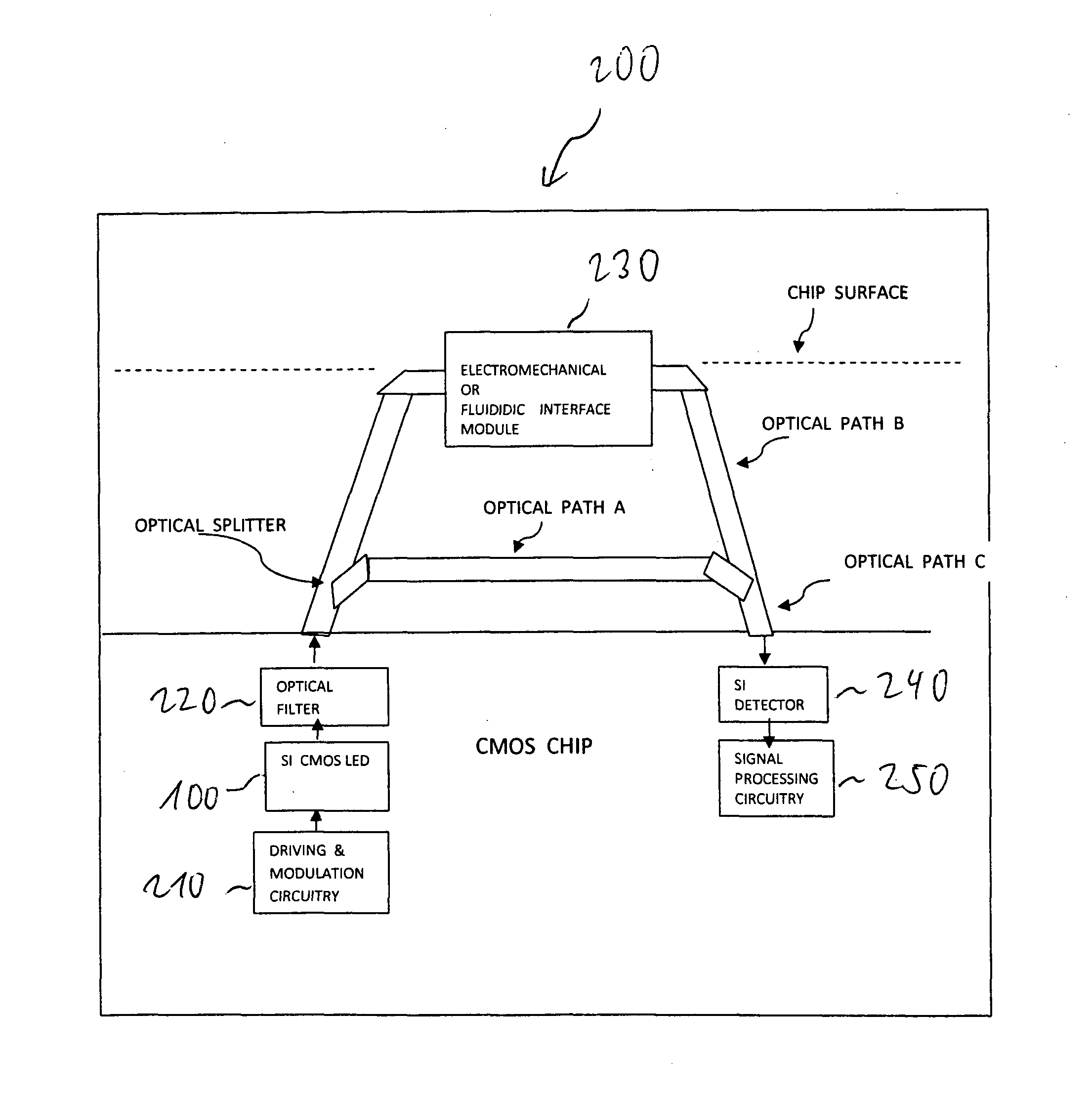
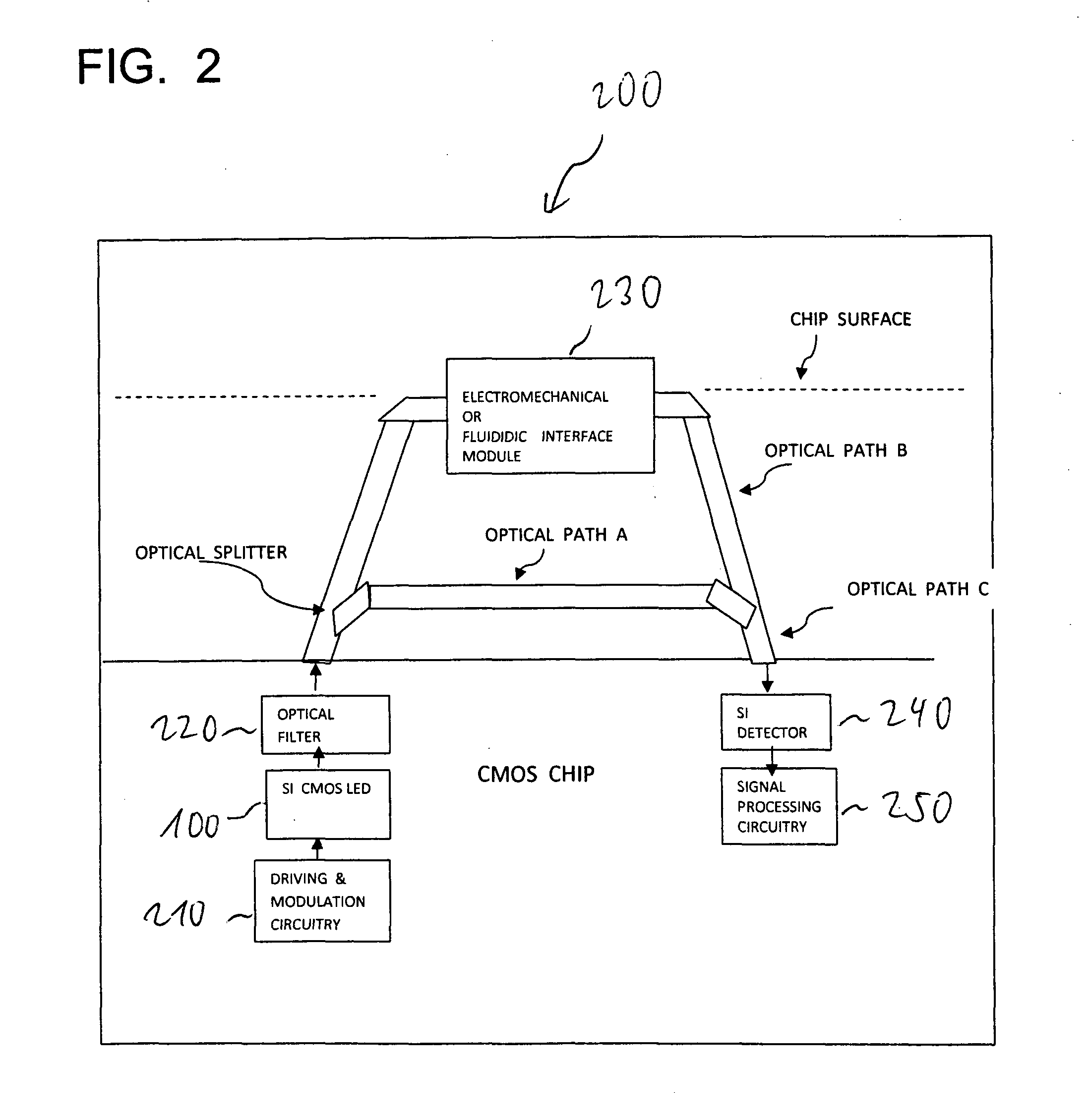
[0014]The sensor may further comprise additional optical filters and a reference optical path section so as to increase the sensitivity of the device for measurements.
[0018]According to a second aspect of the invention, there is provided a method of creating a silicon LED based sensor, wherein: enhanced light emission is created through enhanced secondary excitation processes in the silicon itself; or enhanced light emission is created through enhanced secondary excitation processes in secondary bodies having a high photonic yield and by placing the second body within reach of the secondary body; and utilizing this light emission to sense physical or fluidic change parameters as detected by creating a secondary optical path arrangement which interfaces closely with the environment and creates enhanced detection of the physical changes through either intensity modulation or phase contrast techniques.
[0019]The device utilizes low cost visible light emitters that can be integrated into the system at the chip level at micro-dimensions and that, together with fibre or glass technology and mechanical modules, can provide the measurement of the necessary physical parameter. The key cost competitive advantage in terms of manufacturing costs is achieved with the simplicity of design, simplicity in assembling and in the utilization of low cost integrated circuit integrated LEDs.

Problems solved by technology

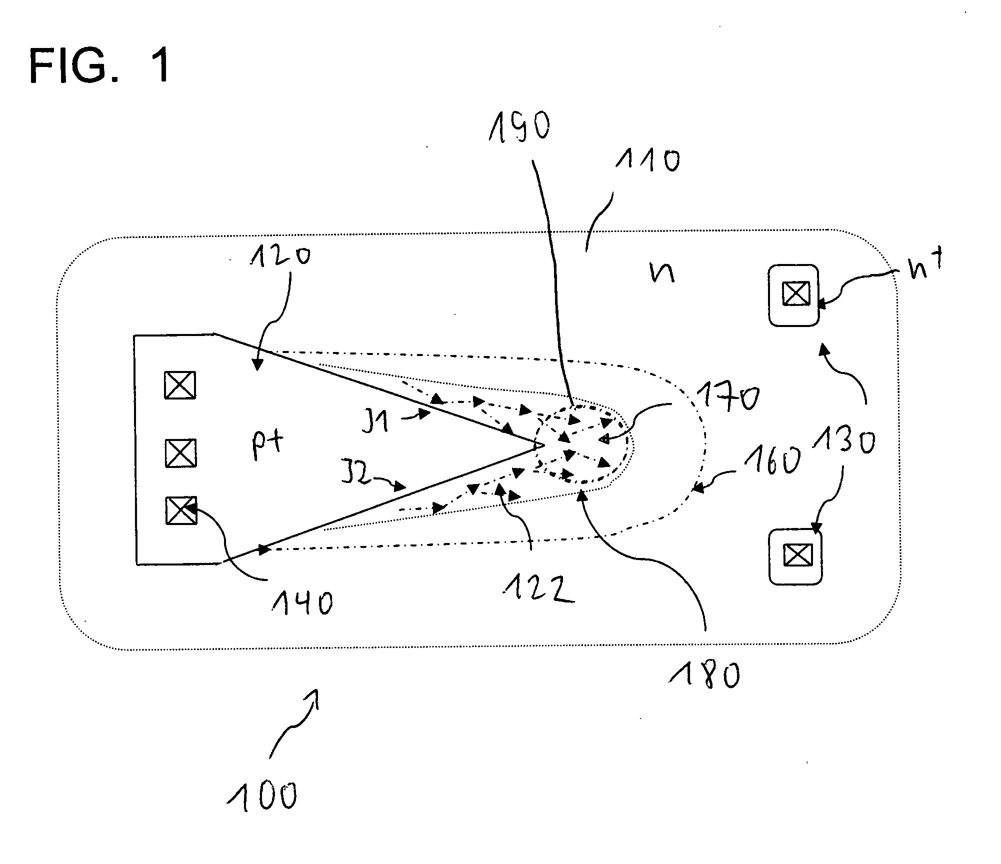
Silicon, however, is an indirect band gap semiconductor material which, unlike a direct band gap semiconductor material, has low photon emission efficiency.
As a result, silicon is considered a poor source of electroluminescent radiation.
However these devices often require complex and sophisticated technology.

Method used


Image

  • CMOS moems sensor device
  • CMOS moems sensor device
  • CMOS moems sensor device

Examples


first embodiment

[0044]FIG. 3 is a schematic diagram showing a hybrid realization the MOEMS device as a preferred first embodiment of the invention, utilizing a mechanical module, an optical module as fabricated in a recess cavity on a CMOS chip hosting the Si LED, optical detection circuitry and appropriate driving and signal processing circuitry. FIG. 3 describes a first hybrid embodiment of the invention fabricating a recess in the CMOS over-layers, and adding various optical and mechanical modules such that a total system is realized using hybrid component and hybrid component assembling means, involving Pick and Placing of components into the recess cavity in a CMOS chip.

[0045]FIG. 3 describes the embodiment of the invention using hybrid approach of the invention. The device consist of three separate modules or bodies viz a semiconductor chip module B1, an optical module or body B2 and a mechanical module or body B3, relative to each other as shown in FIG. 4. An integrated (or embedded) light e...

second embodiment

[0048]FIG. 4 gives the invention using a mixed-hybrid monolithic approach. A recess is manufactured such that the chip surface 400 is sufficiently exposed so as the emit light vertically out of the chip at either a vertical or slanted direction. An appropriate optical filter 220 is fabricated at the chip-recess interface such that only a narrow bandwidth in wavelength of the optical emission of SiLED 100 is transmitted into the recess cavity 410. The electro-mechanical or fluidic interface module 230 is located inside the recess cavity, or partially inside the recess cavity 410 or totally outside the recess cavity. The optical filter 220 may be fabricated using monolithic layer fabrication technology, or it may be pick-and-placed positioned separately into the cavity.

[0049]The optical radiation following path A towards and back from the electromechanical or fluidic interface module 230 is of narrow bandwidth or monochromatic nature which will enhance phase contrast and eventually co...

third embodiment

[0050]FIG. 5 describes a third completely monolithic embodiment of the invention utilizing all CMOS fabrication technology. FIG. 5 is a schematic diagram showing a full monolithic realization the MOEMS device 500 as a preferred third embodiment of the invention, utilizing a mechanical module, as fabricated in a recess cavity on a CMOS chip. The Si LED 100, the wave-guiding circuitry, filtering components and phase contrast enhancement components are all fabricated monolithically as an integral part of the CMOS chip.

[0051]A large area silicon light emitting device supplies sufficient optical power to a monolithically integrated wave guiding system on the chip or section thereof. The optical power is transferred to the waveguides through an appropriate optical coupler 510. The coupled optical radiation in the fibre is then filtered by either a Bragg grating filter 520 or (optional) ring resonator filter 530 (or any other state of the art wave-guiding filtering means) such that a very ...


PUM

PropertyMeasurementUnit
absorption edgeaaaaaaaaaa
wavelengthaaaaaaaaaa

Abstract

The present invention relates to a sensor device. More particularly, the invention relates to a CMOS-based micro-optical-electromechanical-sensor (MOEMS) device with silicon light emitting devices, silicon waveguides and silicon detectors being fabricated using current Complementary Metal Oxide Semiconductor (CMOS) technology or Silicon on Insulator (SOI) technology. According to the invention there is provided a sensor comprising: a Silicon-based light emitting structure; an integrated electro-optical mechanical interface structure that is capable to sense mechanical deflections; an integrated electronic driving and processing circuitry so as to detect physical parameters such as vibration, motion, rotation, acceleration.

Description

INTRODUCTION [0001]The present invention relates to a sensor device. More particularly, the invention relates to a CMOS-based micro-optical-electromechanical-sensor (MOEMS) device with silicon light emitting devices, silicon waveguides and silicon detectors being fabricated using current Complementary Metal Oxide Semiconductor (CMOS) technology or Silicon on Insulator (SOI) technology.BACKGROUND TO THE INVENTION[0002]The vast majority of micro-electronic devices are formed in silicon and, over the last several decades, a substantial effort has been directed to refining the reliability and manufacturability of these devices. As a result, silicon-based microelectronic devices have become dependable and inexpensive commodity items. Particularly, Complementary Metal Oxide Semiconductor (CMOS) technology has become a multi-billion industry providing the basis manufacturing technology for nearly 80° AD of all electronic commodities to society. Furthermore Silicon-on-Insulator (SOI) techno...

Claims


Application Information

Patent Timeline
Patent Type & Authority Applications(United States)
IPC IPC(8): G01N21/59H01L31/18
CPCG01D5/266G01F1/28G01N21/7703H01L27/15G01P15/093G02B6/12004G02B6/4246G01N21/7746G01N21/25H01L27/02
Inventor SNYMAN, LUKAS WILLEM
Owner TSHWANE UNIV OF TECH
Learn More