

Low-molecular compound, polymer, electronic-device material, composition for electronic device, organic electroluminescent element, organic solar cell element, display and lighting
a technology of low-molecular compound and electronic device, which is applied in the direction of thermoelectric device junction materials, solid-state devices, organic semiconductor devices, etc., can solve the problems of difficult superposition of layers by wet film formation methods, reduced driving stability, and reduced solubility of films in organic solvents, so as to improve the solubility of organic solvents, the effect of high solubl
- Summary
- Abstract
- Description
- Claims
- Application Information
AI Technical Summary
Benefits of technology
Problems solved by technology
Method used
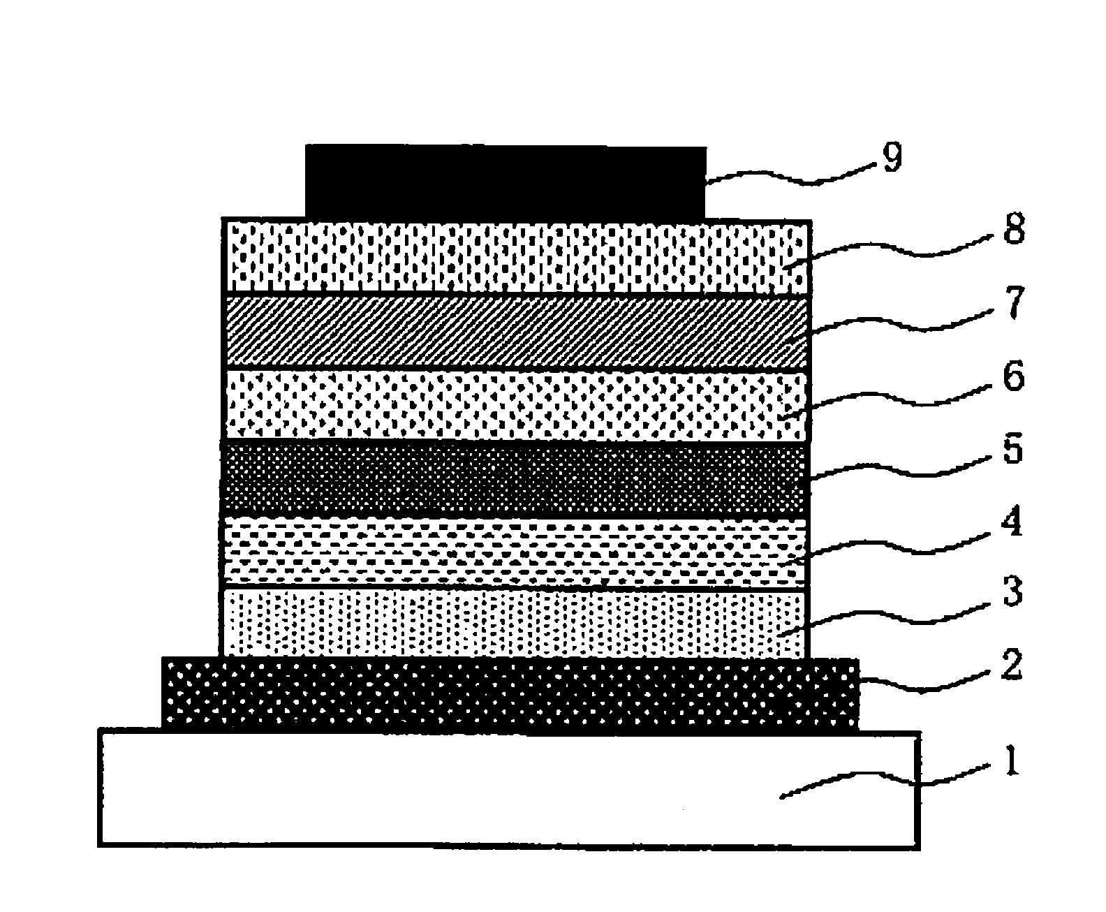
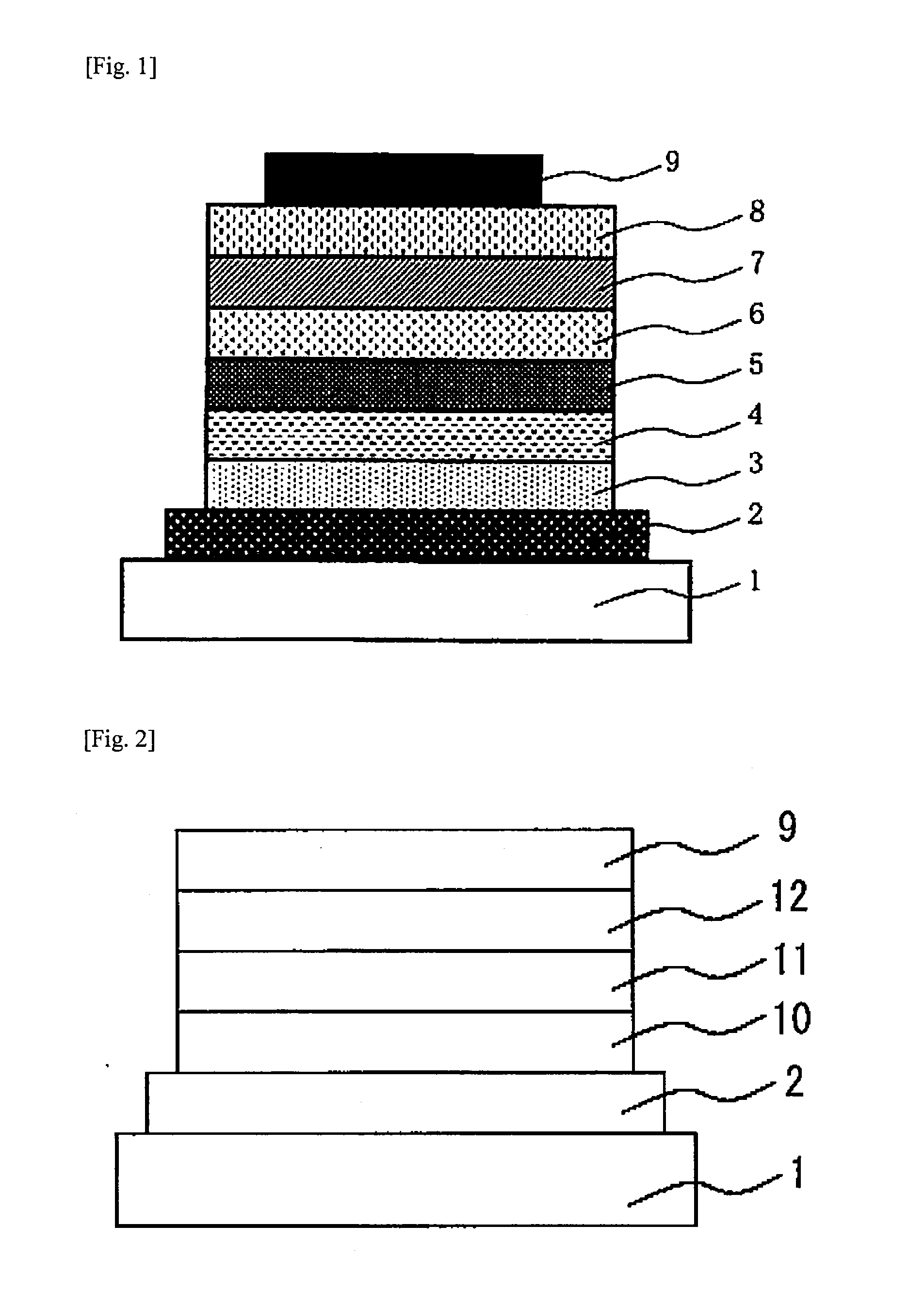
Image

Examples
examples
[0502]The invention will be explained in more detail by reference to Examples. However, the invention should not be construed as being limited to the following Examples unless the invention departs from the spirit thereof.
synthesis examples
Synthesis Example 1
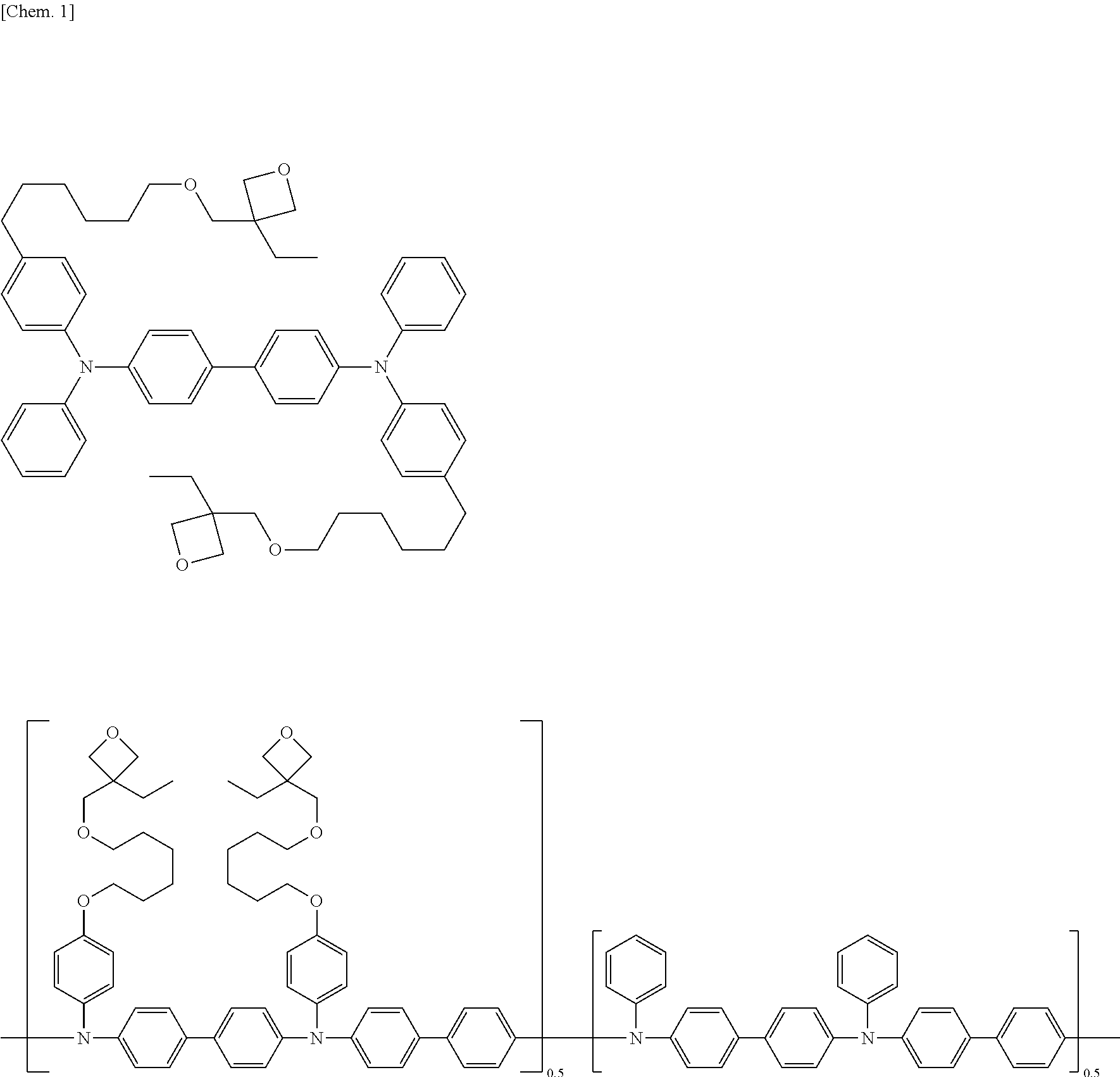
Synthesis of Compound DNOTf
[0503]
[0504]In a nitrogen stream, LiDIAMIN (4.15 g) was added to a solution-state mixture of DNDION (1.0 g) (manufactured by Aldrich Chemical Co.) and tetrahydrofuran (20 mL) with stirring at −78° C., and the resultant mixture was stirred for 1 hour. Thereafter, N-(2-pyridyl)triflimid (7.88 g) was added thereto, and this mixture was stirred at room temperature for 2 days. Fifty milliliters of cold water was added to the reaction solution, and the mixture was extracted with ether. Furthermore, the ether solution was washed with water, dried with MgSO4, and concentrated by an evaporator. The concentrate was purified with a silica column. Thus, DNOTf having a purity of 80% was obtained in an amount of 1.2 g.
[0505](Results of NMR Analysis)
[0506]Compound DNOTf: 1H NMR (CDCl3, 400 MHz) δ 1.6-1.9 (m, 4H), 3.6-3.8 (m, 2H), 6.1-6.2 (s, 2H)
synthesis example 2
Synthesis of Compounds BiNpANDN and NpANDN
[0507]
[0508]Ethanol (3 g), NpANBOR (0.6 g), the DNOTf (0.415 g), sodium carbonate (1.19 g), and water (6 g) were added to toluene (10 g) which had undergone 10-minute nitrogen bubbling, and this mixture was stirred for 30 minutes. Thereafter, tetrakistriphenylphosphinepalladiumdi (0.065 g) was added thereto by hand and dissolved therein, and the resultant solution was stirred at 70° C. for 5 hours. This solution was returned to room temperature, and 100 mL of water was added thereto. The crystals which precipitated were taken out by filtration and washed with ethanol. The crystals were further purified with recycling preparative HPLC Type LC-9204, manufactured by Japan Analytical Industry Co., Ltd. (preparative column, JAIGEL-1H-40). Thus, compound BiNpANDN (0.2 g) and compound NpANDN (0.1 g) were obtained.
(Results of Mass Analysis)
[0509]Mass analysis was conducted using mass spectrometer JMS-700 / MStation, manufactured by JEOL Ltd. (accelera...
PUM
| Property | Measurement | Unit |
|---|---|---|
| temperature | aaaaa | aaaaa |
| temperature | aaaaa | aaaaa |
| boiling point | aaaaa | aaaaa |
Abstract
Description
Claims
Application Information