

Transparent conductive coatings for optoelectronic and electronic devices
a technology of transparent conductive coatings and optoelectronic devices, applied in the direction of conductive materials, chemical vapor deposition coatings, solid-state devices, etc., can solve the problems of low conductivity, high cost, and high cost, and achieve low resistivity, maintain light transmittance, and reduce the effect of resistan
- Summary
- Abstract
- Description
- Claims
- Application Information
AI Technical Summary
Benefits of technology
Problems solved by technology
Method used
Image

Examples
example 1
Printing Holes
[0138]A glass slide was coated by a solvent based silver ink (solvent with dispersed silver nanoparticles) by draw down. Before the total evaporation of the solvent, an aqueous solution was printed on top of the coat by ink-jet printing (MicroFab, 60 um wide nozzle). The solution contained 0.05% of a wetting agent (BYK 348) The printed droplets led to the de-wetting of the silver ink at the printing zone, i.e., to the formation of holes (an area which does not contain the conducting material). The area with holes can be further treated if required to obtain conductivity. For example, if the conducting material is silver nanoparticles, the substrate can be sintered at elevated temperature, or by other chemical means.
example 2
Single Rings
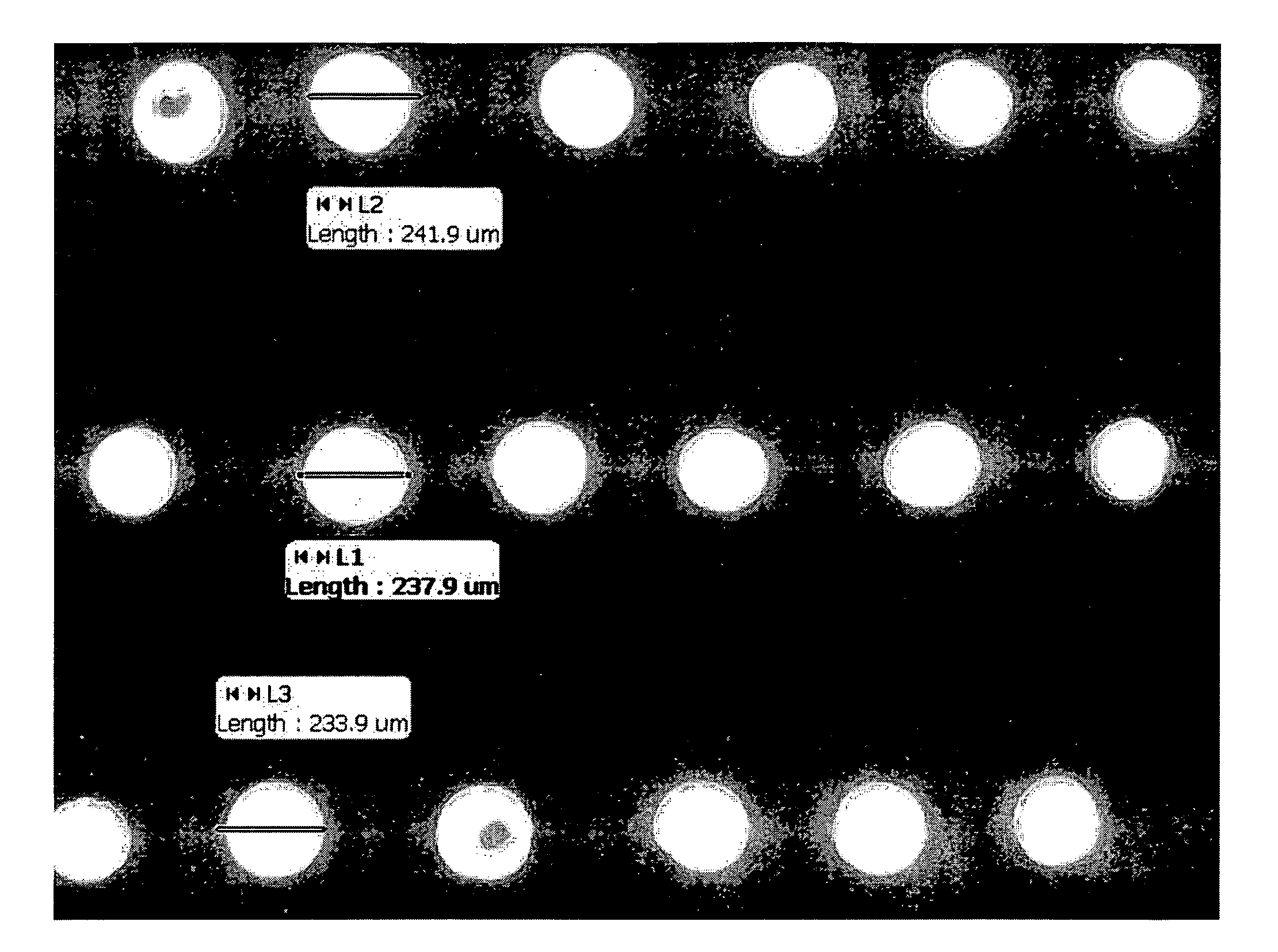
[0139]Single rings with a diameter of ˜150 micrometer were obtained by ink-jetting a silver ink (prepared as described elsewhere [14]) on polyethylene terphthalate (PET) substrate with the single nozzle print-head.
[0140]Silver ink: The aqueous ink contained 0.5 wt % dispersed silver nanoparticles, with a diameter of 5 to 20 nm, stabilized by polyacrylic acid.
[0141]The surface tension of the ink was adjusted to 30 mN / m by the use of Byk®348 (BykCheime). The pH was set to 10 using amino methyl propanol.
[0142]Printing: The printing of the dispersion was performed by Microfab®JetDrive™ III printer with a 60 micrometer wide single nozzle. The applied waveform for all the printing experiments was: voltage 110 V, rise time 3 microsec, echotime 15 microsec, dwell time 30 microsec fall time 5 microsec. As expected, the voltage increased (from the minimal voltage of 20 V), the droplet size increased as well, thus enlarging the ring diameter. Further increase above 110V, was not te...
example 3
Rings Composed of Two Different Metals
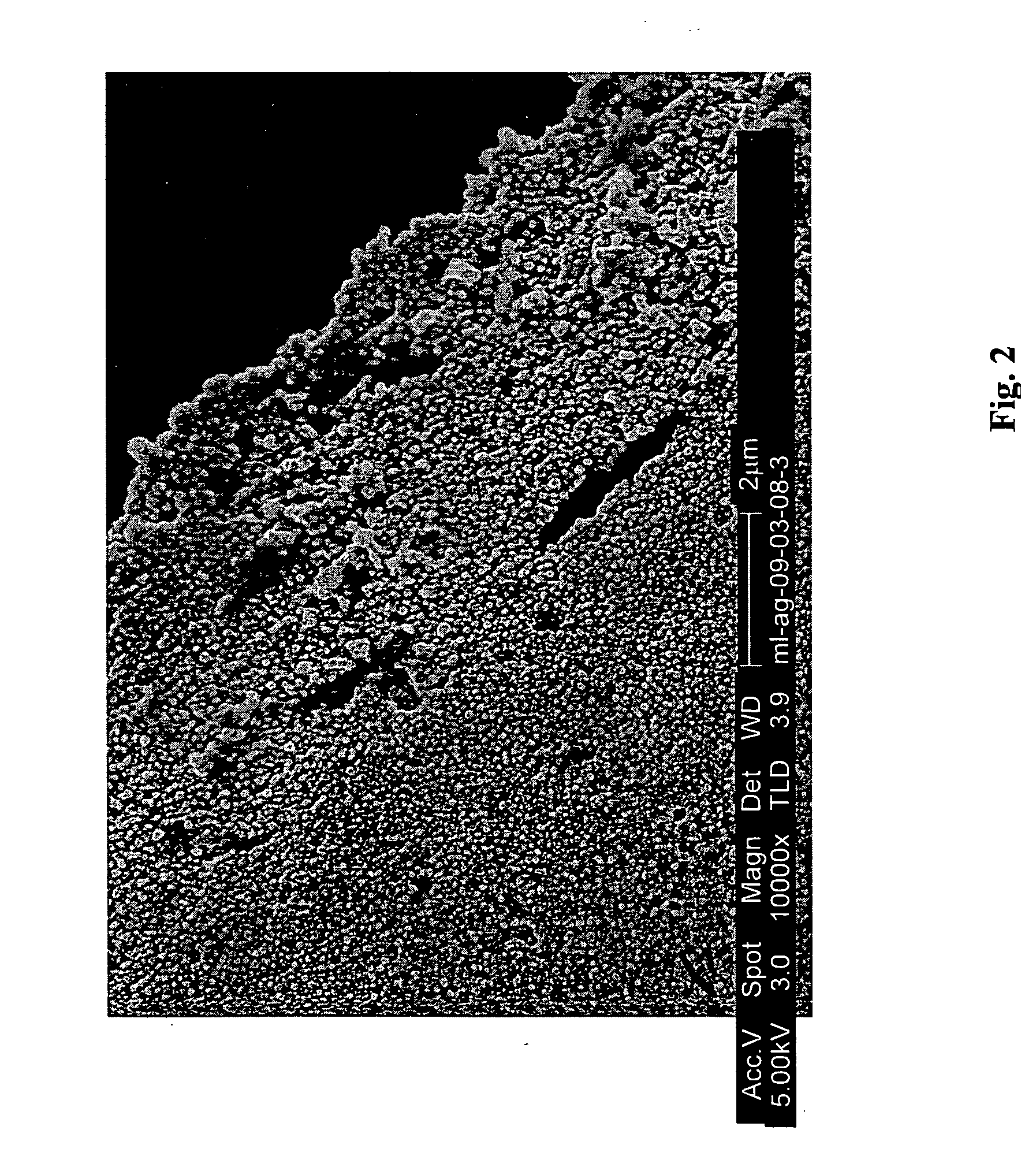
[0148]Two different population of silver and copper NPs were mixed, Ag (˜10 nm) and Cu (˜100 nm) dispersed in water. A 1 μL droplet of this homogenous dispersion was dispensed on a Si substrate. After the evaporation of the water a single ring with a diameter of ˜2 mm was formed. HR-SEM characterization of the ring periphery revealed that the rim is composed of two separate rims (FIG. 2), each rim is consisted mainly of one type of metallic NP; the larger particles (Cu) were at the outer rim while the inner rim consisted mainly of the smaller particles (Ag). Therefore, this approach enables formation of rings composed on different materials.
PUM
| Property | Measurement | Unit |
|---|---|---|
| Length | aaaaa | aaaaa |
| Length | aaaaa | aaaaa |
| Length | aaaaa | aaaaa |
Abstract
Description
Claims
Application Information