

Resist composition and patterning process
- Summary
- Abstract
- Description
- Claims
- Application Information
AI Technical Summary
Benefits of technology
Problems solved by technology
Method used
Image

Examples
example
[0198]Examples of the invention are given below by way of illustration and not by way of limitation. The abbreviation “pbw” is parts by weight. Me stands for methyl.
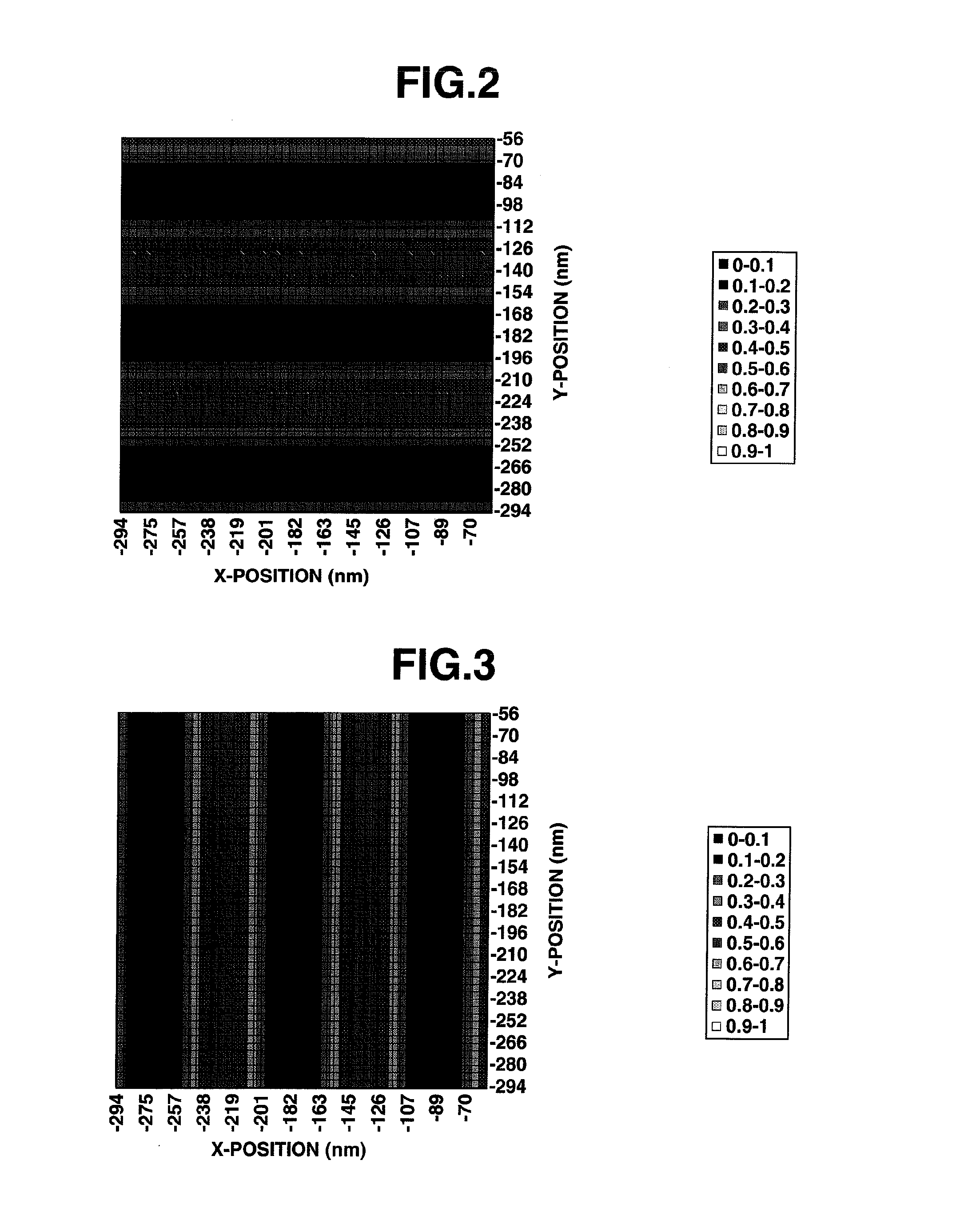
[0199]For all polymers, Mw and Mn are determined by GPC versus polystyrene standards using tetrahydrofuran solvent. For pattern profile observation, a top-down scanning electron microscope (TDSEM) S-9380 (Hitachi High Technologies Corp.) was used.
synthesis example
[0200]Various polymers (Polymers 1 to 16 and Comparative Polymers 1 and 2) for use in resist compositions were prepared by combining suitable monomers, effecting copolymerization reaction in tetrahydrofuran solvent, pouring into methanol for crystallization, repeatedly washing with hexane, isolation, and drying. The polymers were analyzed by 1H-NMR to determine their composition and by GPC to determine Mw and dispersity Mw / Mn.
Preparation of Resist Composition and Protective Film-Forming Composition
[0201]A resist composition in solution form was prepared by dissolving a polymer (Polymers 1 to 16, Comparative Polymers 1 and 2) and components in solvents in accordance with the formulation of Tables 1 and 2. A protective film-forming composition in solution form was prepared by dissolving a polymer (TC Polymer) and additive in solvents in accordance with the formulation of Table 3. The solutions were filtered through a Teflon® filter with a pore size of 0.2 μm.
[0202]The components are i...
examples 3-1 , 3-2
Examples 3-1, 3-2 & Comparative Example 3-1
ArF Lithography Patterning Test 3
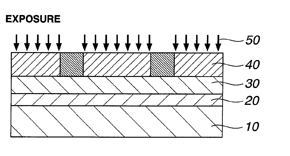
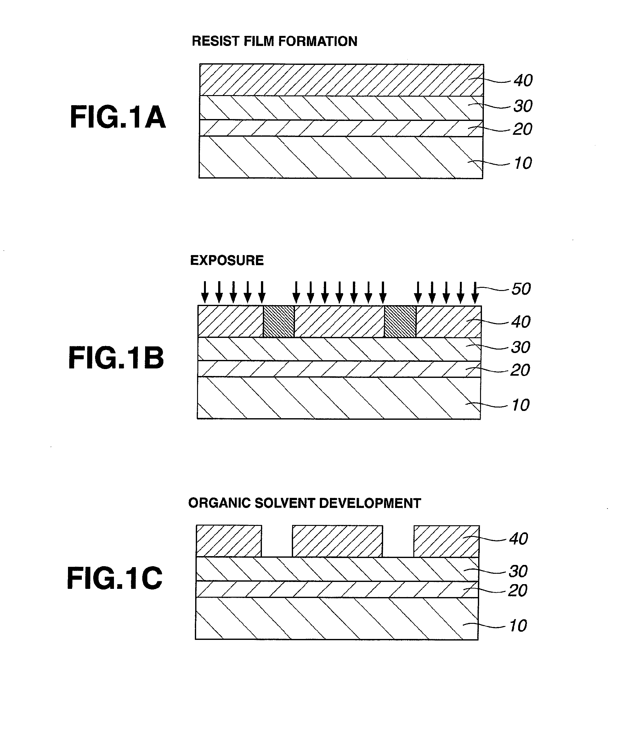
[0212]On a substrate (silicon wafer), a spin-on carbon film ODL-50 (Shin-Etsu Chemical Co., Ltd.) having a carbon content of 80 wt % was deposited to a thickness of 200 nm and a silicon-containing spin-on hard mask SHB-A940 having a silicon content of 43 wt % was deposited thereon to a thickness of 35 nm. On this substrate for trilayer process, the resist composition (Resist 2-15, 2-16, or Comparative Resist 2-4) in Table 2 was spin coated, then baked on a hot plate at 100° C. for 60 seconds to form a resist film of 100 nm thick. The protective film-forming composition TC-1 in Table 3 was spin coated on the resist film and baked at 90° C. for 60 seconds to form a protective film (or topcoat) of 50 nm thick.
[0213]Using an ArF excimer laser immersion lithography scanner NSR-610C (Nikon Corp., NA 1.30, a 0.98 / 0.78, cross-pole opening 20 deg., azimuthally polarized illumination), exposure was performed through a...
PUM
 Abstract
Description
Claims
Application Information