Crosslinkable composition

a crosslinking composition and composition technology, applied in the field of crosslinking compositions, can solve the problems of low molecular weight compounds, require high-level molecular design, and cannot be formed in uniform laminated structures, etc., to achieve excellent conductivity, low resistance, and high conductivity

Inactive Publication Date: 2013-01-31
DAICEL CHEM IND LTD
View PDF0 Cites 10 Cited by
  • Summary
  • Abstract
  • Description
  • Claims
  • Application Information

AI Technical Summary

Benefits of technology

[0069]According to the composition of the present invention, since at least one component among an aromatic polycarbonyl compound, an aromatic polyamine, and an aromatic heterocyclic compound has not less than 3 carbonyl groups (reactive groups containing carbonyl group) or amino groups, or not less than 3 unmodified α-carbon positions as functional groups (reactive groups) or reactive sites, the composition forms, while advancing a reaction of these components, a three-dimensional network structure (a crosslinked structure) in which π-conjugated systems are linked. Accordingly, the organic semiconductor formed with the composition has a low resistance and a high conductivity (carrier mobility). In particular, since the reaction easily proceeds, it is presumed that the organic semiconductor comprises one polymer coupled in three-dimensional network structure substantially composed of a π-conjugated system as a whole. The organic semiconductor formed with the composition forms a pseudo or quasi band structure as a whole, and in the carrier transfer mechanism the nonlocalized intramolecular electron transfer takes precedence over the intermolecular electron transfer (hopping). Thus the organic semiconductor has an extremely excellent conductivity. Moreover, since the intermolecular electron transfer is restrained, the electron transfer is not liable to be inhibited due to oxygen, water, and other impurities. Thus, the organic semiconductor formed with the composition functions as a semiconductor even in a purity (not more than 99%) lower than the purity (not less than 99.9%) necessary for the conventional organic semiconductor. Specifically, since the composition to be used in the present invention does not require special purification treatments (such as sublimation purification) which are necessary for the conventional organic semiconductor, the composition can be provided at a lower cost. Moreover, in the organic semiconductor having a three-dimensional network structure, since an absolute position of each component comprising the organic semiconductor is firmly held, each component is immovilized greatly even if an external energy is applied. Thus the change of the layer (or film) quality (e.g., crystallization) is inhibited, and the organic semiconductor has an excellent durability against heat or other factors and prevents shortening of the lifetime of a device formed with the composition. Further, since the organic semiconductor has an excellent solvent resistance, a coating composition containing an organic solvent can directly be applied to the organic semiconductor to form a laminated structure. The polymerizable components (or reactive components) contained in the composition of the present invention are soluble in a solvent, and the composition can be formed into a layer (or film) by a simple method (such as coating). Further, the composition containing an aromatic heterocyclic compound has a higher stability as a coating composition compared with the composition containing an aromatic polyamine and is useful for forming an organic semiconductor at a low temperature. The characteristics of the organic semiconductor (for example, conductivity and band gap) can easily be controlled by coordinating the species or amount of the polymerizable components (or reactive components).
[0070]Further, since the organic semiconductor of the present invention forms a pseudo or quasi band structure as a whole and is handled in the same manner as an inorganic semiconductor, the organic semiconductor easily forms a hybrid (or composite) with an inorganic semiconductor. In the organic-inorganic hybrid semiconductor, the organic semiconductor is combined with an inorganic semiconductor having a high carrier transfer to improve a photoelectric conversion efficiency, for example, in an application such as solar cell.

Problems solved by technology

These low molecular weight compounds, however, require high-level molecular design.
Moreover, although the intermolecular electron transfer (hopping) is required because of a low molecular weight thereof, sometimes the hopping does not occur depending on the molecular vibration influenced by heat or voltage, and the decrease of conductivity cannot be avoided.
Further, since such a low molecular weight compound is inferior in solvent resistance, a uniform laminated structure cannot be formed by further applying a coating composition containing an organic solvent on a layer containing the low molecular weight compound.
The high molecular weight compound, however, has a rigid molecule structure and is insoluble in a solvent.
Thus it is difficult to form the compound into a layer (or a film) by a simple method (such as coating).
According to this document, however, since an organic semiconductor is obtained by vapor deposition polymerization of the dialdehyde compound and the diamino compound, the ratio of both components cannot accurately be controlled, and thus it is difficult to form a uniform layer.
Further, since the polyazomethine is a linear polymer, the resulting organic semiconductor is insufficient in conductivity, solvent resistance, and durability.
In the crosslinking reaction, however, since the molecules are coupled through a dialkyl ether, the conductivity is insufficient as the whole molecule.
These polymers are therefore insufficient in conductivity, solvent resistance, and durability.
The organic semiconductor, however, strongly binds an electron and an electron hole compared with an inorganic semiconductor, and has an extremely low photoelectric conversion efficiency.
Although the combination of the organic semiconductor and the inorganic semiconductor is also suggested, a high photoelectric effect cannot be achieved yet due to a low conductivity of the organic semiconductor as described above.

Method used


Image

  • Crosslinkable composition
  • Crosslinkable composition
  • Crosslinkable composition

Examples


example 1

(1) Preparation of Composition (Coating Composition)

[0264]In a 6-ml sample bottle, 16.2 mg of 1,3,5-triformylbenzene (manufactured by NARD INSTITUTE, LTD.) and 29.0 mg of tris(4-aminophenyl)amine were added, and these compounds were dissolved in 860 mg of N,N-dimethylacetamide. This mixture was filtered through a filter having a pore size of 0.2 μm to prepare a composition (a coating composition).

(2) Production of Organic Semiconductor Layer

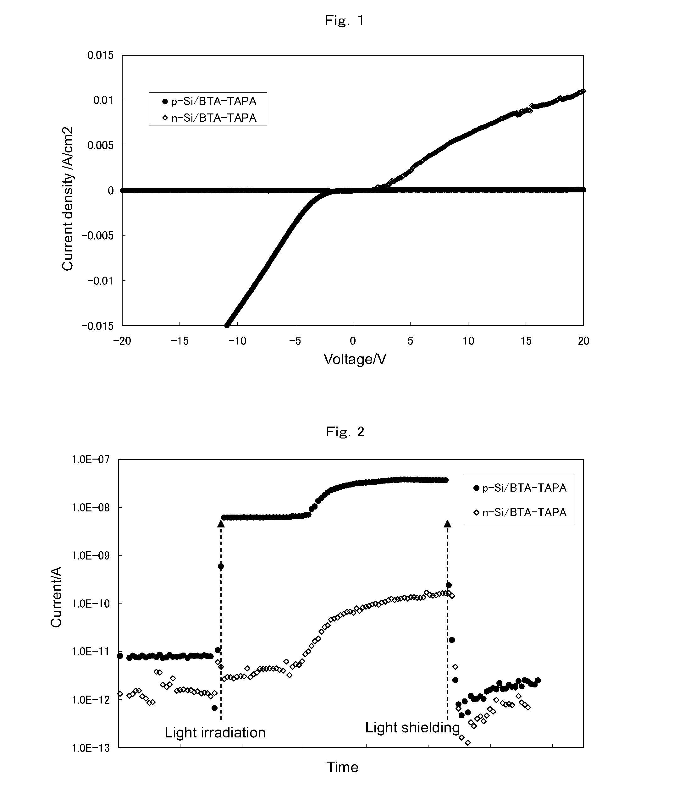
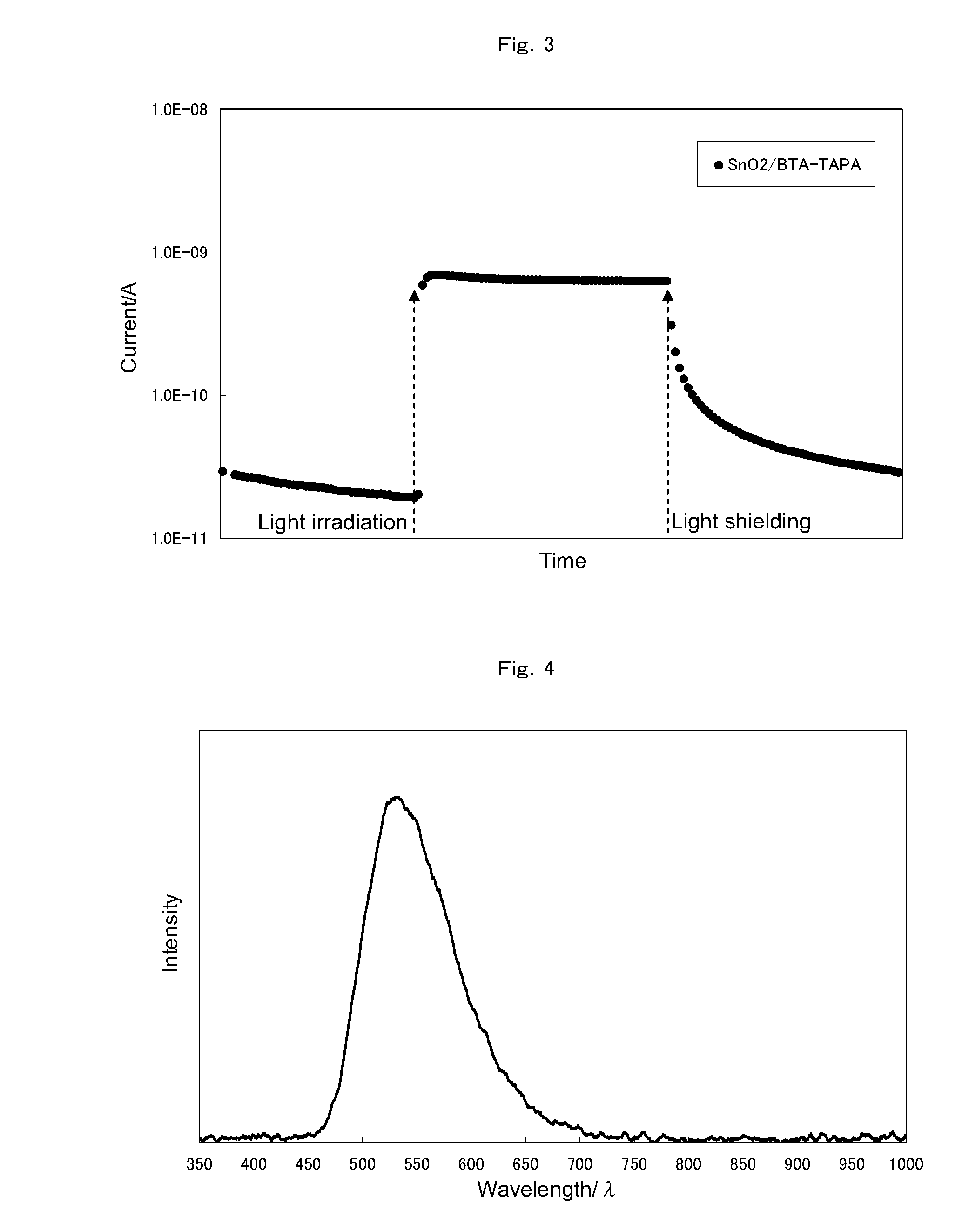
[0265]The composition obtained in the step (1) was applied to a substrate by spin coating to produce a thin layer and then subjected to heat treatment at 300° C. for 1 hour under a nitrogen atmosphere to give an organic semiconductor layer (hereinafter, referred to as BTA-TAPA).

(3) Structure of Organic Semiconductor Layer

[0266](3-1) Solubility in Organic Solvent

[0267]A silicon wafer (or glass plate) was used as a substrate, and a BTA-TAPA layer was produced according to the method of the step (2). The resulting layer was insoluble in N,N-dimethyl...

example 2

(1) Preparation of Composition (Coating Composition)

[0276]In a 6-ml sample bottle, 16.2 mg of 1,3,5-triformylbenzene (manufactured by NARD INSTITUTE, LTD.) and 29.4 mg of 2,7-diaminofluorene were added, and these compounds were dissolved in 1400 mg of N,N-dimethylacetamide. This mixture was filtered through a filter having a pore size of 0.2 μm to prepare a composition (a coating composition).

(2) Production of Organic Semiconductor Layer

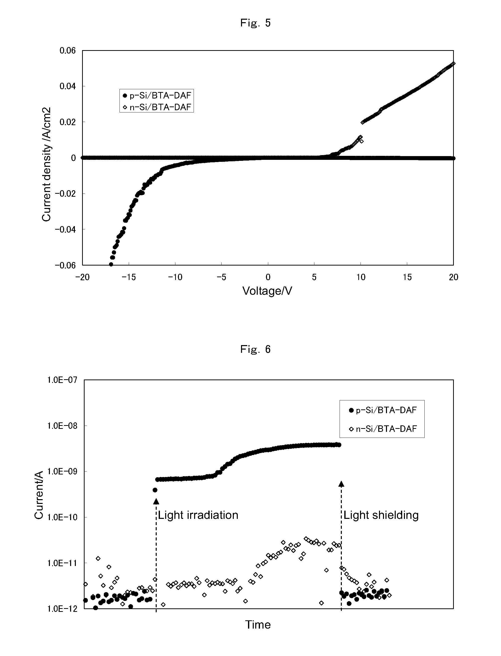
[0277]Using the composition obtained in the above step (1), an organic semiconductor layer (hereinafter, referred to as BTA-DAF) was obtained in the same manner as in Example 1.

(3) Structure of Organic Semiconductor Layer

[0278](3-1) Solubility in Organic Solvent

[0279]A BTA-DAF layer was produced in the same manner as in Example 1. The resulting layer was insoluble in N,N-dimethylacetamide and proved to have a three-dimensional network structure.

[0280](3-2) Band Gap

[0281]The UV-Vis spectrum of the BTA-DAF layer was measured in the same manner as in Ex...

example 3

(1) Preparation of Composition (Coating Composition)

[0286]In a 6-ml sample bottle, 16.2 mg of 1,3,5-triformylbenzene (manufactured by NARD INSTITUTE, LTD.) and 34.8 mg of 1,3-diaminopyrene were added, and these compounds were dissolved in 165 C mg of N,N-dimethylacetamide. This mixture was filtered through a filter having a pore size of 0.2 μm to prepare a composition (a coating composition).

(2) Production of Organic Semiconductor Layer

[0287]Using the composition obtained in the above step (1), an organic semiconductor layer (hereinafter, referred to as BTA-13DAPy) was obtained in the same manner as in Example 1.

(3) Structure of Organic Semiconductor Layer

[0288](3-1) Solubility in Organic Solvent

[0289]A BTA-13DAPy layer was produced in the same manner as in Example 1. The resulting layer was insoluble in N,N-dimethylacetamide and proved to have a three-dimensional network structure.

[0290](3-2) Band Gap

[0291]The UV-Vis spectrum of the BTA-13DAPy layer was measured in the same manner ...


PUM

PropertyMeasurementUnit
crosslinkableaaaaaaaaaa
aromaticaaaaaaaaaa
weightaaaaaaaaaa

Abstract

To provide a composition (e.g., a coating composition) useful for forming an organic semiconductor having excellent conductivity, solvent resistance, heat resistance, durability, and other properties, and an organic semiconductor formed with the composition.The composition comprises an aromatic polycarbonyl compound having a carbonyl group as a reactive site, and at least one aromatic reactive component selected from an aromatic polyamine having an amino group as a reactive site, and an aromatic heterocyclic compound having a plurality of unmodified α-carbon positions, as reactive sites, each of which is adjacent to a hetero atom of a heterocycl thereof. When the aromatic reactive component is an aromatic heterocyclic compound, the aromatic polycarbonyl compound is an aromatic polyaldehyde compound. Use of the composition in which at least one component of the aromatic polycarbonyl compound and the aromatic reactive component has not less than 3 reactive sites per molecule forms an organic semiconductor having a three-dimensional crosslinked structure.

Description

TECHNICAL FIELD[0001]The present invention relates to a crosslinkable composition for providing excellent conductivity, solvent resistance, heat resistance, durability, and other properties [in particular, a composition (e.g., a coating composition) useful for forming an organic semiconductor] and an organic semiconductor or the like formed with the composition.BACKGROUND ART[0002]As organic semiconductors, a low-molecular-weight type and a high-molecular-weight type are known. For example, as a low-molecular-weight-type organic semiconductor component, Japanese Patent Application Laid-Open Publication No. 2004-346082 (JP-2004-346082A, Patent Document 1) discloses a tertiary amine compound represented by the following formula (1), and other compounds, and discloses that the tertiary amine compound having at least one group having an electron donor chemical structure and an electron acceptor chemical structure in a molecule thereof can improve the cohesive force and control the molec...

Claims


Application Information

Patent Timeline
Patent Type & Authority Applications(United States)
IPC IPC(8): H01B1/12C07D209/88C07D333/18H01L51/40C07F5/02C07D333/24C08F34/04H01L51/30C07C251/24C07D207/323
CPCB82Y10/00C09B69/109H01L51/0036H01L51/0039H01L51/0043H01L51/0047H01L51/0054H01L51/4253H01L51/5048C09B69/101C09B69/102C09B69/105C09B69/106C09B69/108H01L51/0035H10K85/115H10K85/111H10K85/215H10K85/151H10K85/113H10K85/622H10K30/30H10K50/14H10K10/484
Inventor FUKUI, KAZUHISAFUNAKI, YOSHINORINOBUTANI, MAMI
Owner DAICEL CHEM IND LTD
Why Eureka
Try Eureka