Nanopore Sensor Comprising A Sub-Nanometer-Thick Layer

Active Publication Date: 2013-02-14
ZHEJIANG UNIV
View PDF3 Cites 43 Cited by
  • Summary
  • Abstract
  • Description
  • Claims
  • Application Information

AI Technical Summary

Benefits of technology

[0022]One of key elements of the present invention is the sub-nanometer-thick functional layer having a nanopore extending through this functional layer. The sub-nanometer-thick functional layer is made of a layered insulating material. Since the sub-nanometer sensitive functional layer can be thinner than the spacing between two adjacent nucleotides in a DNA or RNA strand, the single-base resolution requirement for identifying individual bases in a single-stranded DNA or RNA can be accomplished. The sensitive functional layer of the present invention is suitable for a low cost, rapid DNA sequencing based on ionic current blockade. Employing a sub-nanometer-thick functional layer in the nanopore sensor of the present invention overcomes the technical difficulties in achieving the single-base resolution. The fabrication of the sub-nanometer-thick functional layer is quite simple and can be accomplished by known methods such as mechanical exfoliation of bulk materials, chemical vapor deposition, surface segregation, and chemical reaction. Moreover, the sub-nanometer-thick functional layer is thermally and chemically stable and is iner

Problems solved by technology

In other words, about 15 bases can pass through the nanopore at the same time, and thus it cannot meet the single-base resolution requirement for genome sequencing.
However, due to the honeycomb structure of graphene, nanopore sensors made from graphene membranes suffer from la

Method used


Image

  • Nanopore Sensor Comprising A Sub-Nanometer-Thick Layer
  • Nanopore Sensor Comprising A Sub-Nanometer-Thick Layer
  • Nanopore Sensor Comprising A Sub-Nanometer-Thick Layer

Examples


Example

Embodiment 1: Synthesis and Transfer of boron nitride (h-BN) Membrane

[0058]Synthesis of boron nitride membrane on Cu foil by chemical vapor deposition (CVD): after cleaning and polishing a 25 μm-thick Cu foil, the resulting Cu foil was put into an ultrahigh vacuum chamber (1×10⁻⁸ torr) and thermally treated at 750° C. under an Ar / H2 (˜20 vol % H2) atmosphere for approximately 120 min. The temperature was increased to 950° C., and the Cu foil was treated at this temperature for another 30 min. After the thermal treatment, the Ar / H2 flow was stopped and a mixed gas of B3N3H6 and N2 was fed into the chamber for 20 min to afford a monolayer h-BN (FIG. 5).

[0059]After forming the monolayer h-BN, a 500 nm-thick polymethylmethacrylate (PMMA) layer was spin-coated on the h-BN surface. The Cu was then etched away by putting the PMMA-coated h-BN membrane / Cu stack into a ferric nitrate solution. The Cu substrate was separated from the PMMA / h-BN membrane stack to afford a PMMA / h-BN membrane stac...

Example

Embodiment 2: Fabrication of Nanopore in h-BN Membrane

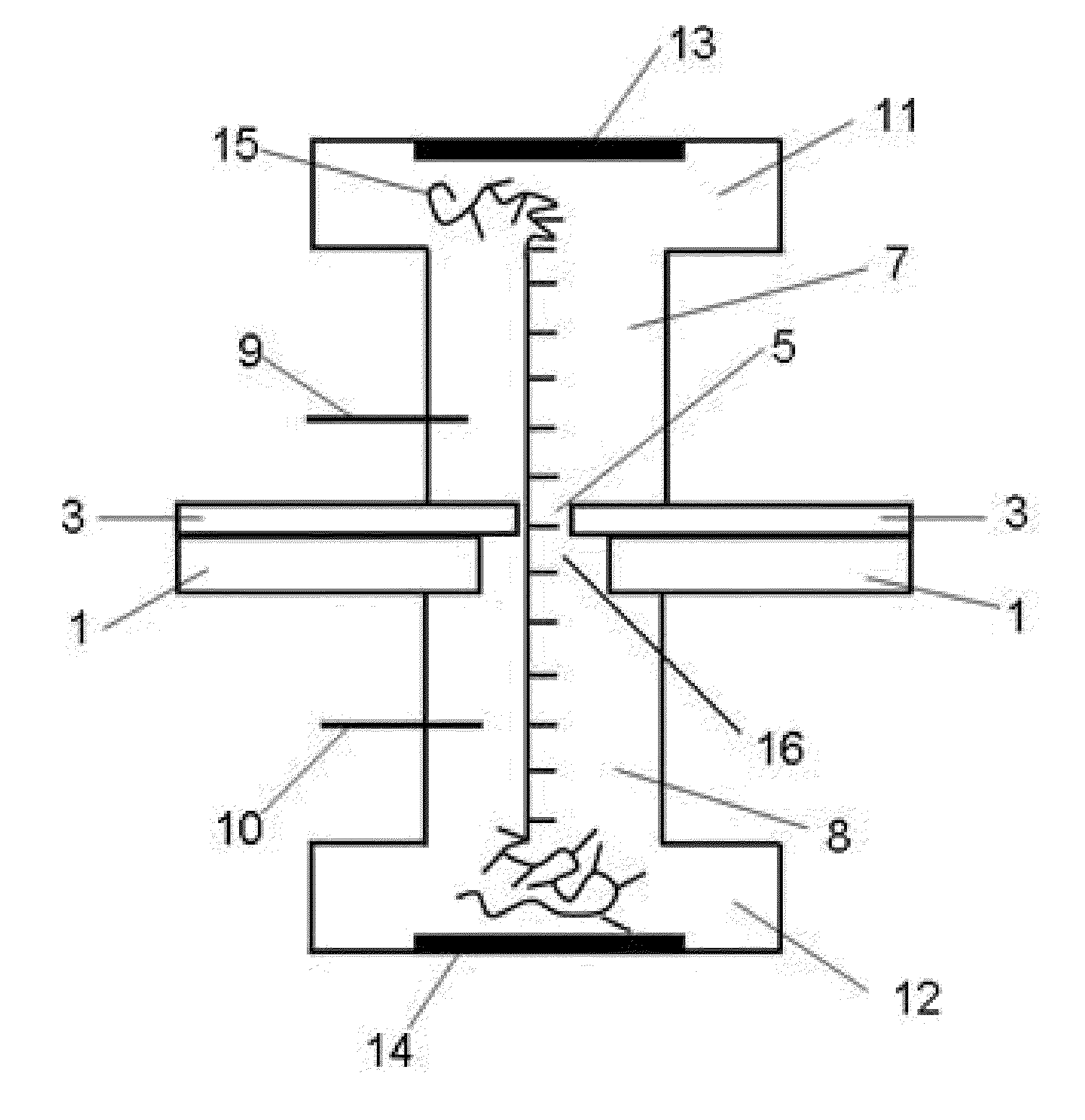
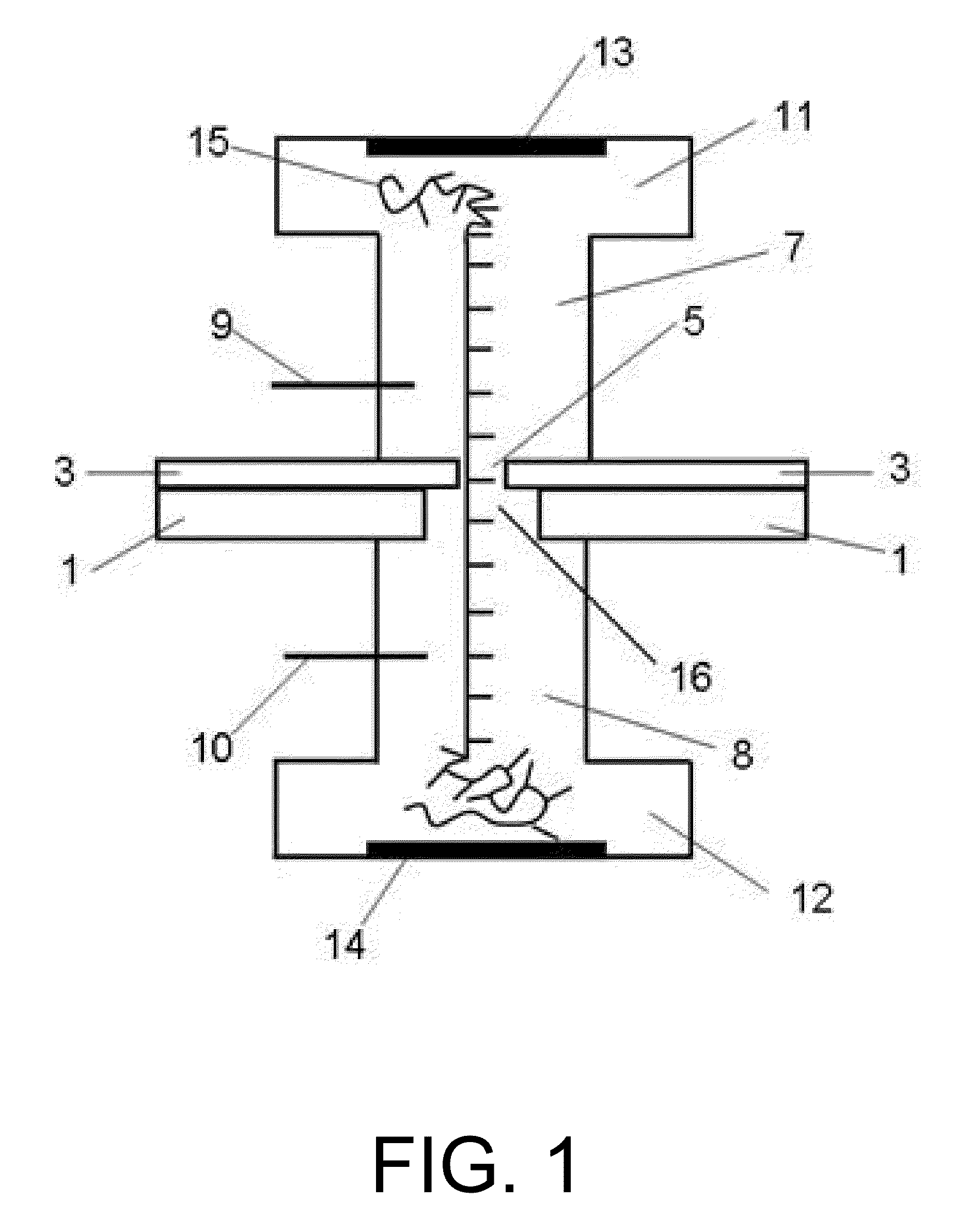
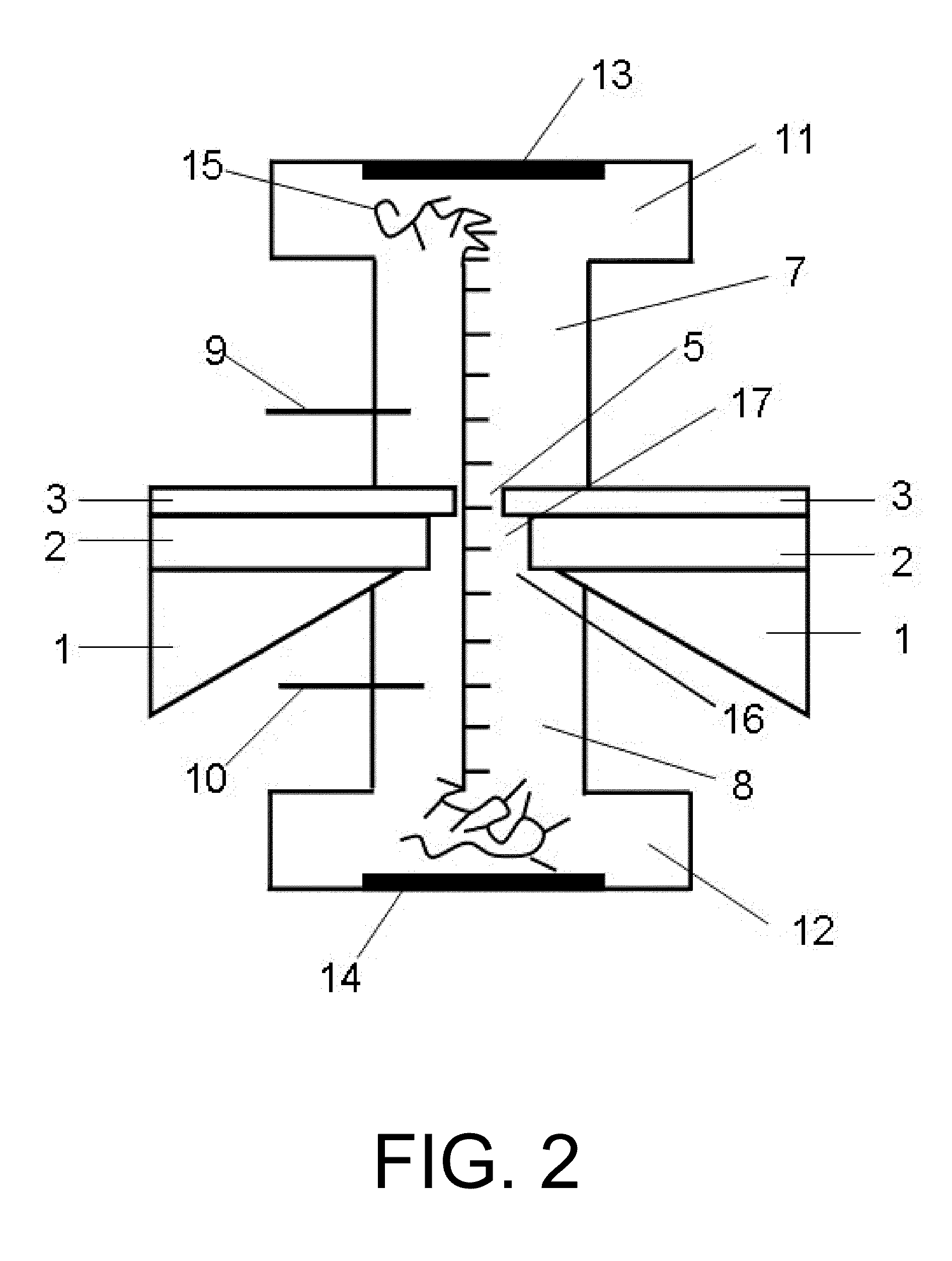
[0060]Referring to the fabrication steps shown in FIG. 6, insulating layer comprising a 30 nm-thick Si3N4 layer is disposed on a 50 nm-thick SiO2 layer on a 600 μm-thick single crystal Si substrate. The Si3N4 was used as the first insulating layer 2, and the SiO2 / Si was used as the substrate 1 (FIG. 6a).

[0061]Using photolithography and lift-off techniques, a circular-shaped opening 16 having a diameter of 80 μm was formed by etching through the SiO2 / Si substrate was done by using a KOH solution to etch patterned region of the Si layer and using a HF buffer solution to etch patterned region of the SiO2 layer, (FIG. 6b).

[0062]Using electron beam lithography and SF6 plasma reactive ion etching techniques, a square-shaped opening 17 (2 μm×2 μm) extending through the Si3N4 layer was formed in the laminated insulating layer (FIG. 6c).

[0063]The synthesized monolayer h-BN was transferred onto the Si3N4 layer as the sub-nanometer-thick f...

Example

Embodiment 3: Synthesis and Transfer of Graphene Membrane

[0067]The graphene was prepared by CVD method: a 100 nm-thick Ni catalyst layer was first formed on a SiO2(300 nm) / Si substrate. The resulting Ni / SiO2 / Si stack was put into an ultrahigh vacuum chamber (1×10⁻⁵ torr), and then thermally treated at 1,000° C. under H2 (1×10⁻⁵ torr) atmosphere for approximately 25 min. The temperature was then decreased to 850° C., and a CH4 gas was fed (100 sccm) into the chamber for 10 min. After that, the temperature was decreased to room temperature at a cooling rate of 20° C. / m i n to afford a graphene membrane with a thickness of approximately 3.35 nm (i.e., 10-layer graphene) on the Ni surface.

[0068]Transfer graphene membrane: a 500 nm-thick PMMA was spin-coated on the surface of the synthesized graphene membrane. The PMMA-coated graphene / Ni / SiO2 / Si stack was then put into a ferric nitrate solution to etch the Ni layer away so as to separate the PMMA / graphene stack from the SiO2 / Si substrate...


PUM

PropertyMeasurementUnit
Nanoscale particle sizeaaaaaaaaaa

Abstract

A nanopore sensor comprises second electrophoresis electrode or micropump, second fluidic reservoir, second micro-nanometer separation channel, substrate, sub-nanometer-thick functional layer, first micro-nanometer separation channel, first electrophoresis electrode or micropump, and electrophoresis electrode or micropump that are sequentially assembled. An opening and a nanopore are provided through the substrate and the sub-nanometer-thick functional layer, respectively. A first electrode for measuring ionic current is provided in the first micro-nanometer separation channel, and a second electrode for measuring ionic current is provide in the second micro-nanometer separation channel. The present invention provides a simple method to prepare a sub-nanometer functional layer having a nanopore extending through the sub-nanometer-thick functional layer. The pore size is comparable to the spacing between two adjacent bases in a DNA strand required for single-base resolution sequencing. The shape of nanopore overcomes nucleotide conformation effect on the identification as bases translocate through the nanopore.

Description

CROSS-REFERENCE TO RELATED APPLICATION[0001]This application is the national phase application of International application number PCT / CN2011 / 080142, filed Sep. 24, 2011, which claims the priority benefit of China Patent Application No. 201010547393.X, filed Nov. 16, 2010. The above-identified applications are hereby incorporated by reference in their entirety.FIELD OF THE INVENTION[0002]The present invention relates to a nanopore sensor, in particular, to a nanopore sensor with a sub-nanometer-thick functional layer.BACKGROUND OF THE INVENTION[0003]Nanopore can be used to detect and characterize biomolecules such as DNA, RNA and peptide at single molecule level. Nanopore-based single molecule genome sequencing technology needs neither fluorescent marker nor polymerase chain reaction (PCR), rather it directly and rapidly reads base sequence in a DNA strand. Such sequencing technology is expected to greatly reduce the sequencing cost to achieve personalized medicine. There are mainly...

Claims


Application Information

Patent Timeline
IPC IPC(8): G01N27/453
CPCG01N33/48721B82Y15/00C12Q1/6869G01N27/447
Inventor XU, MING-SHENGCHEN, HONGZHENGWU, GANGSHI, MINMINWANG, MANG
Owner ZHEJIANG UNIV
Why Eureka
Try Eureka