Through-substrate optical coupling to photonics chips

a photonics chip and optical coupling technology, applied in the field of optical coupling between a waveguide and a photonics chip, can solve the problems of limited optical i/o real estate available at the chip edge, difficult integration of silicon based lasers or light sources, and difficult introduction of light beams to ics

Active Publication Date: 2013-08-15
IBM CORP
View PDF6 Cites 123 Cited by
  • Summary
  • Abstract
  • Description
  • Claims
  • Application Information

AI Technical Summary

Benefits of technology

[0011]In an embodiment, a metallic reflective layer is formed in the metal-dielectric stack adjacent the diffractive coupling elements to redirect light to the diffractive coupling elements and therein enhance optical coupling efficiency.
[0019]In an embodiment, a metallic reflective layer is formed in said metal-dielectric stack adjacent the diffractive coupling elements to redirect light to the diffractive coupling elements and therein enhance optical coupling efficiency.
[0026]In an embodiment, the semiconductor body includes at least one groove formed in the second surface of the semiconductor body to reflect light from the diffractive coupling elements into a direction substantially parallel with the first and second surfaces of the semiconductor body to an edge of the semiconductor body, said edge being on a third side of the semiconductor body, between the first and second sides thereof. The fiber array connector comprises one or more mechanical alignment elements to facilitate positioning the fiber array connector adjacent said edge of the semiconductor body in a position aligned to receive the light reflected by said at least one groove.
[0027]Embodiments of the invention provide backside optical coupling from optical waveguides fabricated on the front surface of a photonic chip through the semiconductor substrate. Embodiment of the invention use grating-based near-normal optical coupling schemes disposed on the front waveguide surface in combination with lens elements and alignment features integrated on the back surface of the substrate. In embodiments of the invention, the addition of metal minors disposed over the grating structure is used to enhance efficiency. The grating coupler is also compatible with polarization diversity schemes, mode-matching to specific optical fiber mode dimensions, and 2-D fiber array coupling.

Problems solved by technology

One device, however, that has been difficult to integrate is a silicon based laser or light source.
Unfortunately, introducing a light beam to an IC can often be difficult.
This edge coupling approach may suffer from limited real estate available at the chip edge for optical I / O, limited I / O density limited to 1-D fiber arrays, and additional complexity (such as fiber tapers, lenses, etc.) required for interfacing the unmatched mode field diameters at the chip edge and fiber facet.
However, the intrinsic trade-off in the grating couplers between coupling efficiency and bandwidth, as well as a fundamental coupling efficiency limit of less than unity, plagues systems seeking to implement this technology.
Additionally, the standard approach of coupling from the top of the photonic device layer is not compatible with CMOS-processing, which includes several layers of metals and dielectrics above the photonic device layer.
In this implementation, the optical beam passes through the chip substrate, but the optical properties of the substrate are not leveraged for increased coupling performance.
However, evanescent coupling schemes, rather than grating-based coupling schemes, are used, which require a costly thinning of the buried oxide layer to less than 250 nm (typically 1 to 3 um).

Method used


Image

  • Through-substrate optical coupling to photonics chips
  • Through-substrate optical coupling to photonics chips
  • Through-substrate optical coupling to photonics chips

Examples


Embodiment Construction

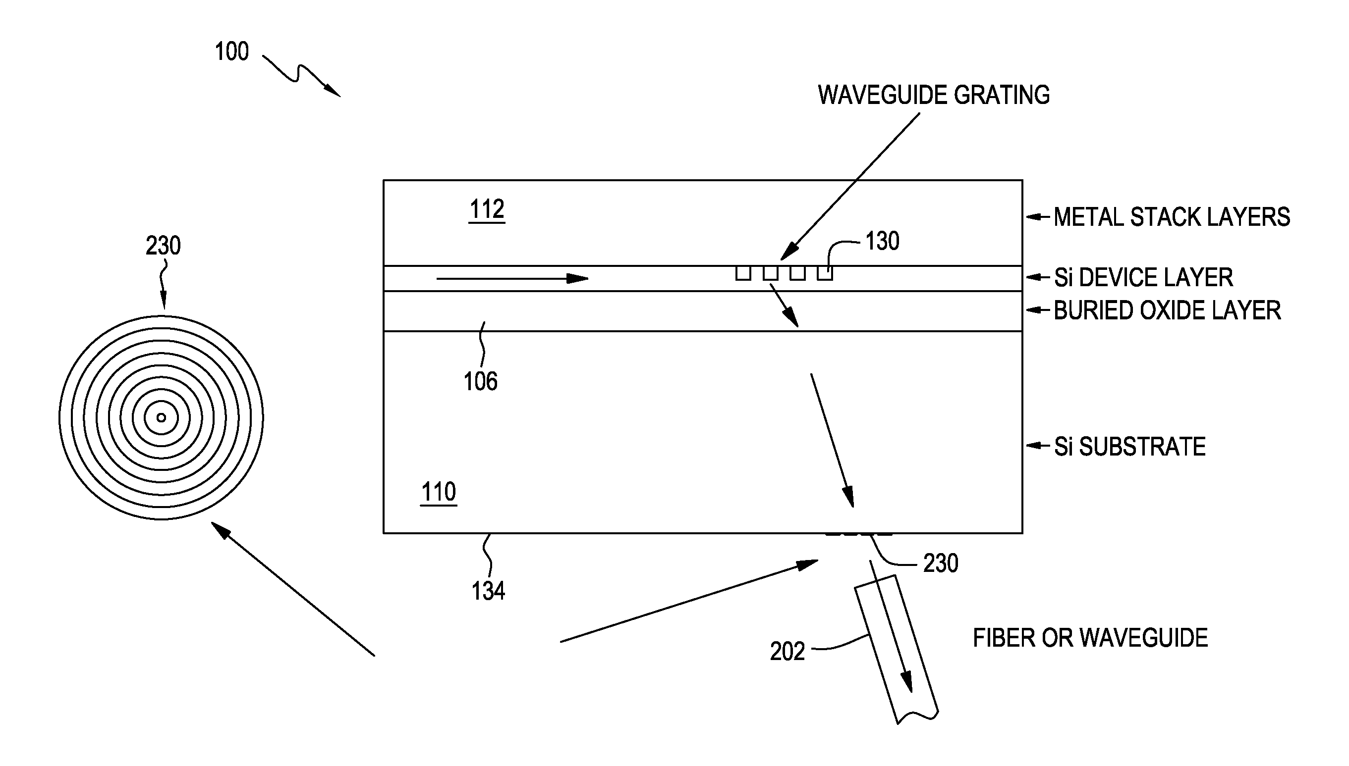
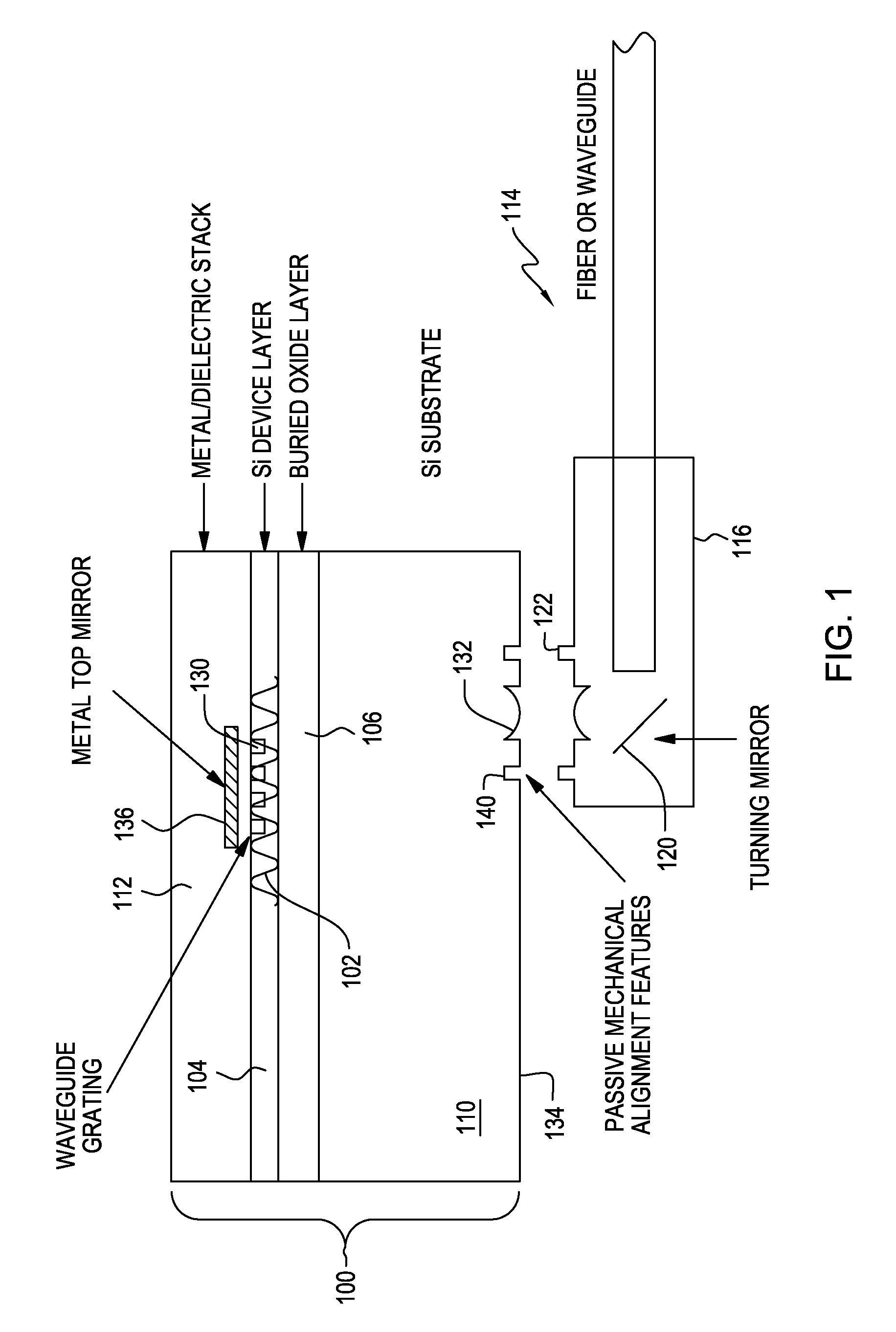
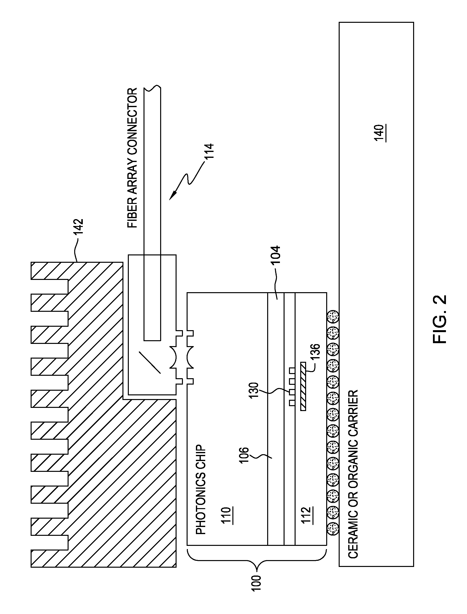
[0040]Embodiments of the invention provide an optical coupling structure that receives a light beam and couples the beam into a waveguide. In a reverse manner, the optical coupling structure may also move light away from the waveguide and out of an optoelectronic IC. The methods of fabricating such an optical structure described below implement a variety of conventional semiconductor processes and combinations thereof, which include: lithography, etching, thin-film deposition, and anti-reflective coatings. Moreover, some of the embodiments also include methods that may employ conventional wafer to wafer attachment / bonding processes.

[0041]For simplicity, the description below and related figures describe an optical coupling structure that includes a silicon-based waveguide that consists of single crystalline silicon layer. In alternative embodiments the waveguide may be polycrystalline silicon and it may also comprise multiple layers with specific characteristics for each individual ...


PUM


Abstract

An optoelectronic integrated circuit for coupling light to or from an optical waveguide formed in an optical device layer in a near-normal angle to that layer. In an embodiment, the integrated circuit comprises a semiconductor body including a metal-dielectric stack, an optical device layer, a buried oxide layer and a semiconductor substrate arranged in series between first and second opposite sides of the semiconductor body. At least one optical waveguide is formed in the optical device layer for guiding light in a defined plane in that device layer. Diffractive coupling elements are disposed in the optical device layer to couple light from the waveguide toward the second surface of the semiconductor body at a near-normal angle to the defined plane in the optical device layer. In an embodiment, an optical fiber is positioned against the semiconductor body for receiving the light from the coupling elements.

Description

STATEMENT REGARDING FEDERALLY SPONSORED RESEARCH OR DEVELOPMENT[0001]This invention was made with government support under Contract No. H90011-08-C-0102 (NOBS) (Defense Advanced Research Projects Agency (DARPA)). The government has certain rights in the invention.BACKGROUND OF THE INVENTION[0002]This invention generally relates to optoelectronic integrated circuits, or photonics chips, and more specifically, to optical coupling between a waveguide and a photonics chip.[0003]Optoelectronic integrated circuits (ICs) include both electronic and optical elements within a single chip. Typical electronic elements include field effect transistors, capacitors, and resistors; and typical optical elements include waveguides, optical filters, modulators, and photodetectors. Within a given optoelectronic IC, some of the electronic elements may be dedicated to handling tasks such as data storage and signal processing. Other electronic elements may be dedicated to controlling or modulating the op...

Claims


Application Information

Patent Timeline
Patent Type & Authority Applications(United States)
IPC IPC(8): G02B6/12H01L33/58
CPCH01L25/167G02B6/4214G02B6/124G02B6/29323H01L2924/0002H01L2924/00G02B6/12002G02B6/136G02B6/30G02B6/32G02B6/3652G02B2006/12104G02B6/12G02B6/12004G02B6/13G02B6/305G02B6/34G02B6/43
Inventor DOANY, FUADLEE, BENJAMIN G.SCHOW, CLINT L.
Owner IBM CORP
Why Eureka
Try Eureka