Method for manufacturing sputtering target, method for forming oxide film, and transistor

a technology of oxide film and sputtering target, which is applied in the direction of metallic material coating process, inorganic chemistry, crystal growth process, etc., can solve the problems of low crystallinity of oxide semiconductor film, defect generation at the interface between stacked oxide semiconductor film, oxygen vacancy or dangling bond, etc., to improve the electrical characteristics of a semiconductor device or the like and improve the reliability of a semiconductor device including an oxide semiconductor film

Active Publication Date: 2014-08-28
SEMICON ENERGY LAB CO LTD
View PDF4 Cites 30 Cited by
  • Summary
  • Abstract
  • Description
  • Claims
  • Application Information

AI Technical Summary

Benefits of technology

[0022]In accordance with one embodiment of the present invention, a method for manufacturing a sputtering target with which an oxide semiconductor film with a small amount of defects can be formed can be provided. In accordance with one embodiment of the present invention, an oxide semiconductor film with a small amount of defects can be formed. In accordance with one embodiment of the present invention, electrical characteristics of a semiconductor device or the like including an oxide semiconductor film can be improved. In accordance with one embodiment of the present invention, reliability of a semiconductor device including an oxide semiconductor film can be improved.

Problems solved by technology

An oxide semiconductor film with low crystallinity is likely to include defects such as oxygen vacancies or dangling bonds.
In the case where stacked oxide semiconductor films formed using sputtering targets with different compositions have different crystallinities, defects are generated at the interface between the stacked oxide semiconductor films.
Defects included in an oxide semiconductor film or defects combined with hydrogen or the like might cause carrier generation and change electrical characteristics of the oxide semiconductor film.
This results in poor electrical characteristics of a transistor and causes an increase in the amount of change in electrical characteristics of the transistor, typically the threshold voltage, due to a change over time or a stress test (e.g., a bias-temperature (BT) stress test or a BT photostress test).

Method used


Image

  • Method for manufacturing sputtering target, method for forming oxide film, and transistor
  • Method for manufacturing sputtering target, method for forming oxide film, and transistor
  • Method for manufacturing sputtering target, method for forming oxide film, and transistor

Examples


embodiment 1

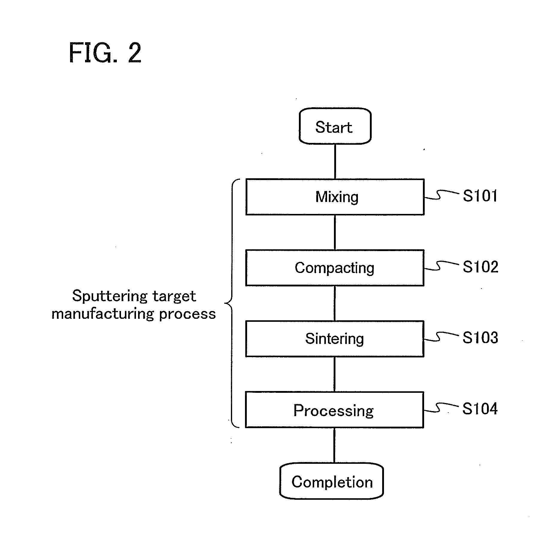
[0072]In this embodiment, a method for manufacturing a sputtering target will be described.

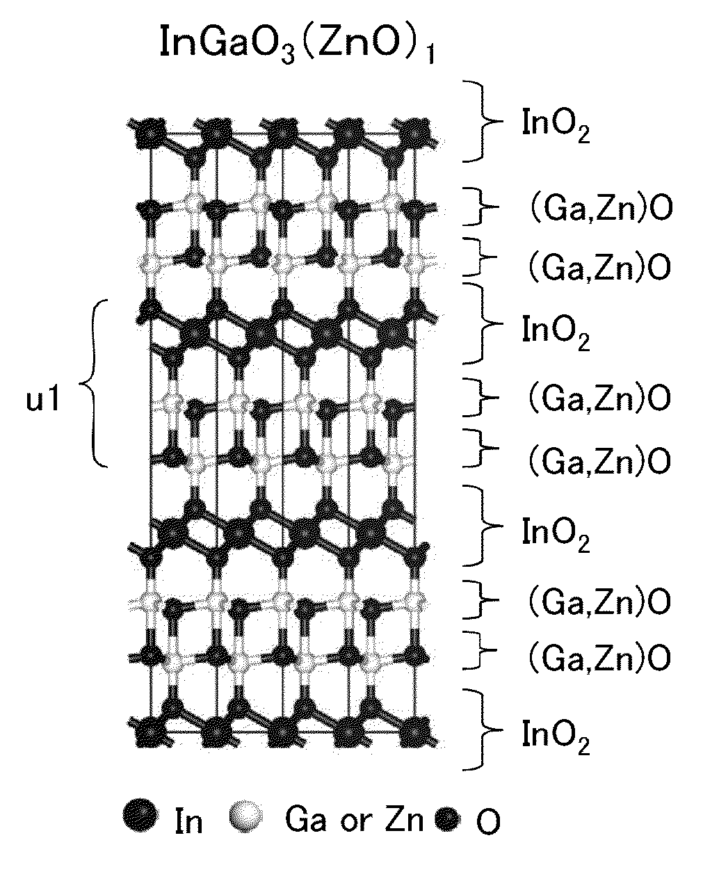
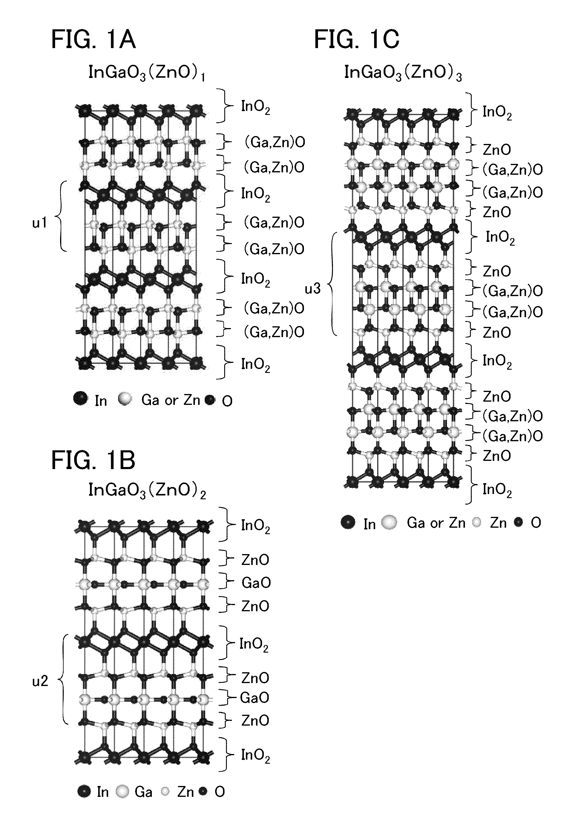
[0073]First, homologous compounds represented by InMO3(ZnO)m (M represents Al, Ti, Ga, Y, Zr, La, Cs, Nd, or Hf, and m is a natural number) are described. The homologous compounds represented by InMO3(ZnO)m have the same crystal structure as LuFeO3(ZnO)m having a layered structure in which LuO2− layers and (FeZnm)Om+11+ layers are stacked regularly and alternately, with the space group R−3m when m is an odd number and with the space group P63 / mmc when m is an even number. Note that InMo3(ZnO)m (m=1) is also referred to as a YbFe2O4 structure. Such a crystal structure is referred to as a homologous structure. Note that in this specification, crystal structures are basically in hexagonal representation.

[0074]Next, crystal structures of homologous compounds are described using InGaO3(ZnO)m as a typical example of InMO3(ZnO)m. FIGS. 1A to 1C illustrate crystal structures of InGaO3(ZnO)m where m=1 ...

embodiment 2

[0122]A method for forming an oxide film using the sputtering target manufactured in Embodiment 1 will be described in this embodiment with reference to FIGS. 4A to 4C, FIGS. 5A to 5F, FIGS. 6A to 6C, FIGS. 7A and 7B, FIGS. 8A to 8C, FIGS. 9A to 9C, FIGS. 10A and 10B, FIG. 11, FIGS. 12A to 12C, FIGS. 13A and 13B, FIGS. 14A to 14C, FIG. 15, FIGS. 16A to 16C, FIGS. 17A to 17C, and FIGS. 18A and 18B. Here, a description is given using an In—Ga—Zn oxide as a typical example of an In-M-Zn oxide (M represents Al, Ti, Ga, Y, Zr, La, Cs, Nd, or Hf).

[0123]FIGS. 4A to 4C, FIGS. 8A to 8C, FIGS. 14A to 14C, FIGS. 16A to 16C, FIGS. 17A to 17C, and FIGS. 18A and 18B are schematic diagrams illustrating a sputtering process in a deposition chamber of a deposition apparatus. Note that the deposition chamber of the deposition apparatus will be briefly described in this embodiment and will be described in detail in Embodiment 3.

[0124]As illustrated in FIG. 4A, a substrate stage 12 and a sputtering tar...

embodiment 3

[0220]In this embodiment, a deposition apparatus for depositing a highly crystalline oxide film will be described with reference to FIGS. 19 and 20.

[0221]First, a structure of a deposition apparatus that hardly allows the entry of impurities into a film during deposition will be described with reference to FIGS. 19 and 20.

[0222]FIG. 19 is a schematic top view of a single wafer multi-chamber deposition apparatus 4000. The deposition apparatus 4000 includes an atmosphere-side substrate supply chamber 4001 including a cassette port 4101 for storing substrates and an alignment port 4102 for performing alignment of substrates, an atmosphere-side substrate transfer chamber 4002 through which a substrate is transferred from the atmosphere-side substrate supply chamber 4001, a load lock chamber 4003a where a substrate is carried in and the pressure is switched from atmospheric pressure to reduced pressure or from reduced pressure to atmospheric pressure, an unload lock chamber 4003b where a...


PUM


Abstract

A method for manufacturing a sputtering target with which an oxide semiconductor film with a small amount of defects can be formed is provided. Alternatively, an oxide semiconductor film with a small amount of defects is formed. A method for manufacturing a sputtering target is provided, which includes the steps of: forming a polycrystalline In-M-Zn oxide (M represents a metal chosen among aluminum, titanium, gallium, yttrium, zirconium, lanthanum, cesium, neodymium, and hafnium) powder by mixing, sintering, and grinding indium oxide, an oxide of the metal, and zinc oxide; forming a mixture by mixing the polycrystalline In-M-Zn oxide powder and a zinc oxide powder; forming a compact by compacting the mixture; and sintering the compact.

Description

BACKGROUND OF THE INVENTION[0001]1. Field of the Invention[0002]The present invention relates to a method for manufacturing a sputtering target, a method for forming an oxide film, and a transistor.[0003]2. Description of the Related Art[0004]Transistors used for most flat panel displays typified by a liquid crystal display device or a light-emitting display device are formed using a silicon semiconductor such as amorphous silicon, single crystal silicon, or polycrystalline silicon provided over a glass substrate. Further, such a transistor employing such a silicon semiconductor is used in integrated circuits (ICs) and the like.[0005]In recent years, attention has been drawn to a technique in which, instead of a silicon semiconductor, a metal oxide exhibiting semiconductor characteristics is used in transistors. Note that in this specification, a metal oxide exhibiting semiconductor characteristics is referred to as an oxide semiconductor.[0006]For example, InGaO3(ZnO)m (m: a natura...

Claims


Application Information

Patent Timeline
Patent Type & Authority Applications(United States)
IPC IPC(8): C01G15/00C23C14/08
CPCC01G15/00C23C14/08C01G15/006C01P2002/32C01P2002/72C01P2002/85C01P2004/04C01P2004/61C01P2004/62C01P2004/64B82Y30/00C23C14/086C23C14/3414H01J37/3429C30B23/08C30B29/22H01J2237/081H01J2237/3322C30B1/04C30B28/02C30B29/68H01J2237/3323H01L21/02565H01L21/02609H01L21/02631H01L29/045H01L29/24H01L29/66969H01L29/7869H01L29/78696
Inventor YAMAZAKI, SHUNPEITSUBUKU, MASASHIOOTA, MASASHIKUROSAWA, YOICHIISHIHARA, NORITAKA
Owner SEMICON ENERGY LAB CO LTD
Why Eureka
Try Eureka