
Method for manufacturing flexible-embedded electrode film using heat-pressure welding transcription

a flexible electrode and transcription technology, applied in the direction of insulating bodies, insulating supports, conductive layers on insulating supports, etc., can solve the problems of many complicated wires on the board, wiring defects may be incurred during the manufacturing process, and electrical shorts between circuit wires, etc., to achieve easy wiring formation, low resistance, and simple process

Inactive Publication Date: 2015-07-30
LG CHEM LTD
View PDF4 Cites 15 Cited by
  • Summary
  • Abstract
  • Description
  • Claims
  • Application Information

AI Technical Summary

Benefits of technology

The present invention provides a method to create a flexible electrode film with a conductive pattern embedded in a plastic film using a simple process. This encourages the formation of wiring with low resistance without the limitations of metal wiring. The method uses thermal and pressure lamination, allowing for a large-area plastic electrode film to be easily manufactured. The buried flexible electrode film is durable, exhibits superior adhesion and minimal surface contamination, resulting in high transmittance and low resistance. It can be used in various applications such as flexible displays, touch panels, solar cells, and flexible printed circuit boards.

Problems solved by technology

Although conventional circuit wires may be composed of a metal wiring pattern formed on an insulating board, when the circuit wires on the insulating board are crossed in the same plane, an electrical short may occur between the circuit wires.
However, forming the multilayer circuit patterns on a circuit board has to be carried out by a series of complicated processes, and thereby wiring defects may be incurred during the manufacturing process.
Also, forming many complicated wires on the board inevitably requires wiring having a smaller line width.
As the width of the wiring decreases, the cross-sectional area thereof is reduced, thus causing problems of high resistance, low power efficiency and heat generation.
However, considerable effort and time are needed to develop materials having resistivity as low as that of conventionally useful metallic materials such as copper, aluminum or silver.
However, indium, mainly contained in ITO, which is a conductive metal oxide, is unsuitable for use in a flexible electrode introduced on a plastic board requiring flexibility due to its high brittleness thereof.
Accordingly, to solve problems with electrodes using ITO, manufacturing techniques using carbon nanotubes or conductive polymer materials are under investigation but still remain in the study stages, and thus the development of the manufacturing process necessary for practical product development needs more time.
Designing a resistance circuit via a short wiring length is difficult to actually implement in a variety of electronic devices.
Moreover, increasing the height of wiring is difficult in terms of processes, and also involves problems of wire breaking and an electrical short between wires.
However, this technique is complicated due to a plurality of processes including pattern engraving, selective filling of the engraved portion (recess) with the conductive material, and forming the conductive film, and makes it difficult to completely remove the conductive material from the portion other than the engraved portion, and unavoidably creates defects in each of the individual processes.
However, this technique is problematic because of complicated processes with the addition of coating and curing of the curable polymer layer, and wet peeling.
Furthermore, in the wet peeling process of the sacrificial layer, the exposure area of the sacrificial layer is small in a lateral direction of the film, and thus the wet dissolution rate may decrease, making it worse to scale up a large-area conductive film.

Method used


Image

  • Method for manufacturing flexible-embedded electrode film using heat-pressure welding transcription
  • Method for manufacturing flexible-embedded electrode film using heat-pressure welding transcription
  • Method for manufacturing flexible-embedded electrode film using heat-pressure welding transcription

Examples


example 1

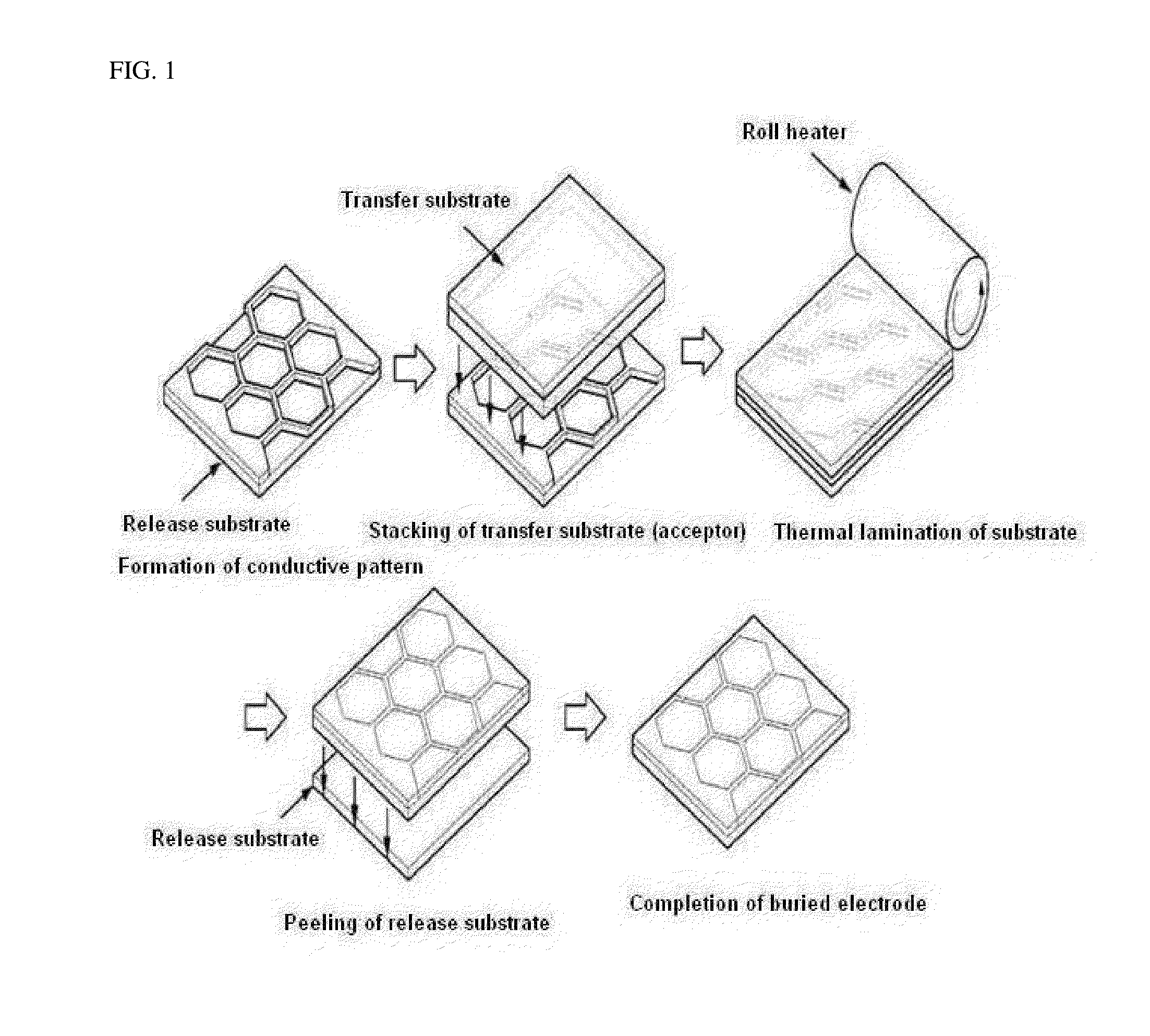
[0100]A PET substrate having a thickness of 180 μm was coated with a 5 mm thick polydimethylsiloxane (PDMS) (SYLGARD 184, available from Dow Corning Corp.) solution (mixing ratio 1:9) and cured at 70° C. for 6 hr, thus preparing a release-substrate. A 150 nm thick Al foil was deposited on the release surface of the release-substrate using an e-beam deposition machine (base pressure: 8×10⁻⁷ torr, working pressure: 5×10⁻⁵ torr, 0.1 Å / s).

[0101]Using an AZ 1518 photoresist, coating, drying, mask photoexposure and development were performed, thus forming a pattern on the Al deposited film.

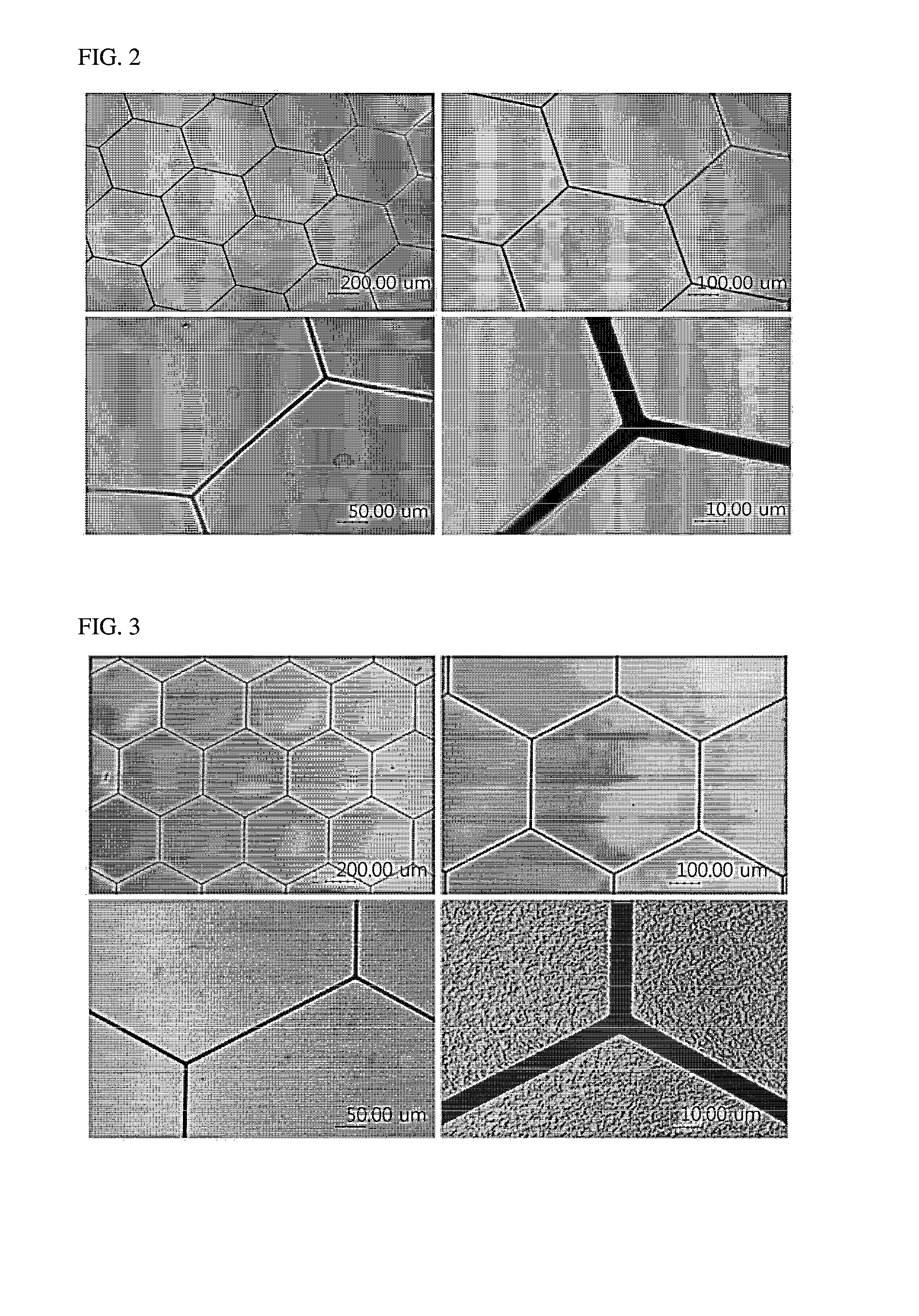
[0102]The formed resist pattern was subjected to wet etching (a phosphoric acid-based Al etching solution) or dry etching (ICP-RIE), thus forming an Al electrode pattern. Based on observation by an optical microscope, the Al electrode pattern was formed as illustrated in FIG. 2.

[0103]On the Al electrode pattern, a 250 μm EVA (Ethylene Vinyl Acetate) film (Pouch laminating film, available from GMP Ltd.) ...

example 2

[0105]A flexible conductive buried electrode film was manufactured in the same manner as in Example 1, with the exception that a 180 μm thick PET substrate was spin-coated with a 1˜5 wt % diluted fluorinated silane (OPTOOL™, available from Daikin Industries, LTD.) solution and dried at 120° C. for 30 min, thus preparing a release-substrate.


PUM

PropertyMeasurementUnit
thicknessaaaaaaaaaa
thicknessaaaaaaaaaa
widthaaaaaaaaaa

Abstract

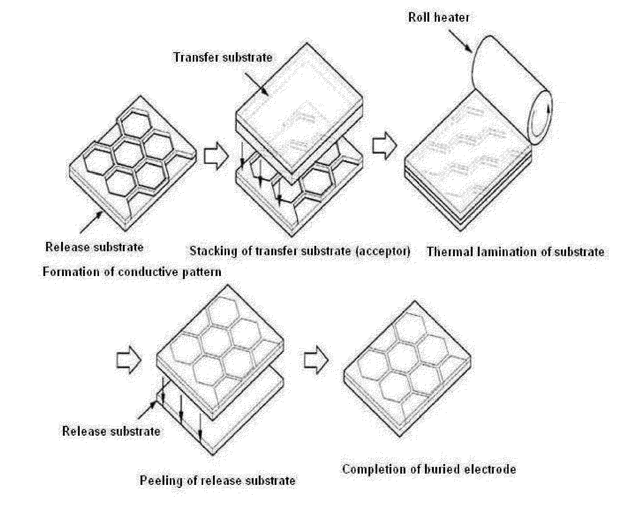
This invention relates to a method of manufacturing a buried flexible electrode film, including 1) preparing a release-substrate; 2) forming a conductive pattern layer on the release-substrate; 3) positioning a transfer-substrate on the conductive pattern layer and then performing thermal and pressure lamination so that the conductive pattern layer formed on the release-substrate is inserted or buried in the surface of the transfer-substrate; and 4) separating the release-substrate and the conductive pattern layer from each other, and to a buried flexible electrode film manufactured thereby.

Description

BACKGROUND OF THE INVENTION[0001]1. Technical Field[0002]The present invention relates to a method of manufacturing a buried flexible electrode film using thermal lamination transfer.[0003]2. Description of the Related Art[0004]With the recent advancement in the electrical and electronic industries, a variety of home appliances and electronic products have been developed. Due to trend for more compact electronic products, thorough research is ongoing to cope with the technical demands for reducing the size and the thickness of such electronic products.[0005]Circuit boards include circuit wires for electrically connecting electrical devices, electronic devices and semiconductor packages. Although conventional circuit wires may be composed of a metal wiring pattern formed on an insulating board, when the circuit wires on the insulating board are crossed in the same plane, an electrical short may occur between the circuit wires. Hence, the circuit board typically includes multilayer ci...

Claims


Application Information

Patent Timeline
Patent Type & Authority Applications(United States)
IPC IPC(8): H05K3/20B32B37/00H05K1/02
CPCH05K3/20H05K1/0284H05K1/0296B32B37/025H05K2201/09036H05K2203/06B32B2305/38B32B2457/08H05K3/207H05K2201/0129H05K2201/0376H05K2201/09681H05K2203/1545H01B5/00H01B5/102H01B5/14H01B5/16H01B13/00H01B17/62H01L31/022425H01L31/022466
Inventor PARK, JEONGHOSHIN, BUGONKIM, JAEJINLEE, JONGBYUNGJUNG, JINMI
Owner LG CHEM LTD
Learn More