Semiconducting Layer Production Process

Inactive Publication Date: 2016-01-14
OXFORD UNIV INNOVATION LTD
View PDF2 Cites 22 Cited by
  • Summary
  • Abstract
  • Description
  • Claims
  • Application Information

AI Technical Summary

Benefits of technology

[0010]The present inventors have developed processes for producing layers of a semiconductor material. They have found that it is possible to produce layers of a semiconductor material formed from particles of the semiconductor material which can show both high surface area and good electronic properties, particularly regarding elec

Problems solved by technology

However, in many cases, it can be difficult to produce a high surface area layer of a semiconductor material which also maintains good electronic properties without resorting to the use of high temperature sintering.
In the case of mesoporous (high surface area) semiconductor

Method used


Image

  • Semiconducting Layer Production Process
  • Semiconducting Layer Production Process
  • Semiconducting Layer Production Process

Examples


example

Mesoporous Layer Production

Low Temperature Solar Cell Assembly:

[0434]This example shows that effective high-surface area (mesoporous) layers of a semiconductor material can be produced at low temperature.

[0435]FTO-coated glass sheets (15 Ωcm−1 Pilkington) were etched with zinc powder and HCl (2M) to obtain the required electrode pattern. The sheets were then washed with soap (2% Hellmanex in water), deionized water, acetone, and methanol, and finally treated under oxygen plasma for 10 minutes.

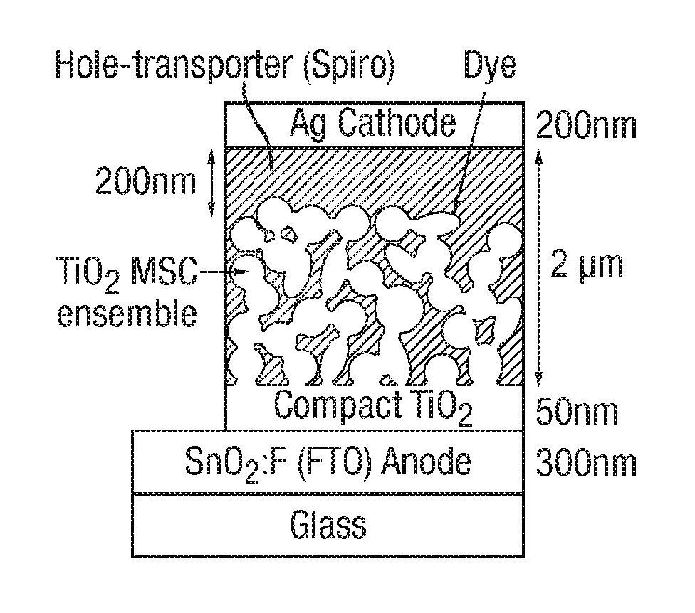
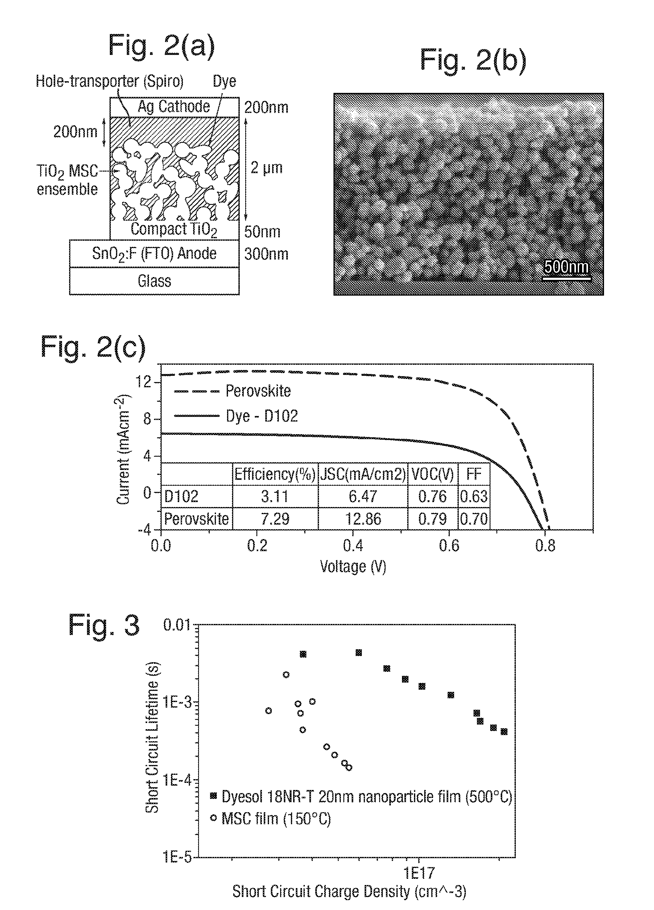
Compact Layer Formation

[0436]A TiO2 compact layer was first deposited by spin-coating on a clean fluorine-doped tin oxide (FTO) coated glass substrate. The compact layer spin-coating solution was prepared by adding 0.71 g titanium isopropoxide and 0.07 g HCl to 8 mL of ethanol. The compact layer was then dried at 150° C. for 30 minutes.

Semiconductor Layer Production

[0437]The TiO2 MSC film ensemble was deposited by spin-coating a solution of MSCs (300 nm crystal size, 50 nm pore size) dispersed ...


PUM


Abstract

The invention provides a process for producing a layer of a semiconductor material, wherein the process comprises: a) disposing on a substrate: i) a plurality of particles of a semiconductor material, ii) a binder, wherein the binder is a molecular compound comprising at least one metal atom or metalloid atom, and iii) a solvent; and b) removing the solvent. The invention also provides a layer of semiconductor material obtainable by this process. In a preferred embodiment, the particles of a semiconductor material comprise mesoporous particles of the semiconductor material or mesoporous single crystals of the semiconductor material. The invention provides a process for producing a compact layer of a semiconductor material, wherein the process comprises: disposing on a substrate i) a solvent, and ii) a molecular compound comprising at least one metal or metalloid atom and one or more groups of formula OR, wherein each R is the same or different and is an unsubstituted or substituted C1-C8 hydrocarbyl group, and wherein two or more R groups may be bonded to each other; and b) removing the solvent. The invention also provides a compact layer of a semiconductor material obtainable by this process. These processes can be effectively performed at temperatures of less than 300° C. Further provided are semiconductor devices comprising either a layer of a semiconductor material or a compact layer of a semiconductor material obtainable by the processes of the invention. The invention also provides a process for producing a semiconductor device.

Description

FIELD OF THE INVENTION[0001]The invention relates to a process for producing a layer of a semiconductor material processed at moderate temperatures. The invention also relates to a process for producing a compact layer of a semiconductor material processed at moderate temperatures. Furthermore, the invention relates to devices comprising layers obtainable by these processes.[0002]The invention also provides a compact layer for a semiconductor device and semiconductor devices comprising said compact layer.BACKGROUND OF THE INVENTION[0003]It is rare to find a contemporary electronic device which does not have as an integral component a semiconductor material in some form or another. In particular, layers of semiconductor materials are near ubiquitous in electronics. These layers may be mesoporous layers or compact layers. Compact layers are typically dense nano- or microcrystalline films.[0004]Increasingly, layers of a semiconductor material displaying a high surface area are finding ...

Claims


Application Information

Patent Timeline
IPC IPC(8): H01G9/20H01L51/42H01L51/00
CPCH01L51/4226H01G9/2031H01L51/0003H01L51/4233H01G9/204Y02E10/549Y02E10/542H10K85/00H10K30/151H10K30/00H10K2102/102H10K85/50H10K30/152H10K71/12
Inventor SNAITH, HENRY JAMESCROSSLAND, EDWARD JAMES WILLIAMSNOEL, NAKITASIVARAM, VARUNLEIJTENS, TOMAS
Owner OXFORD UNIV INNOVATION LTD
Why Eureka
Try Eureka