Nitrogen doped and vacancy dominated silicon ingot and thermally treated wafer formed therefrom having radially uniformly distributed oxygen precipitation density and size

a technology of nitrogen doping and oxygen precipitation, which is applied in the field of vacancy-dominated single crystal silicon ingots, can solve the problems of affecting the yield potential of complex and highly integrated circuit materials, affecting the electronic properties of wafers, and the number of defects in single crystal silicon form, so as to achieve the effect of increasing the density increasing the size of radial bulk micro defects

Active Publication Date: 2016-02-04
GLOBALWAFERS CO LTD
View PDF2 Cites 10 Cited by
  • Summary
  • Abstract
  • Description
  • Claims
  • Application Information

AI Technical Summary

Benefits of technology

[0013]The present disclosure is further directed to a nitrogen-doped CZ silicon crystal ingot. The ingot has a diameter of from about 150 mm to about 450 mm and has a nitrogen concentration of from about 1*1013 nitrogen atoms per cm3 to about 1*1015 nitrogen atoms per cm3. A wafer sliced from the silicon crystal ingot and thermally treated at 780° C. for 3 hours and then at 1000° C. for 16 hours is characterized by an increase in radial bulk micro defect size in a region extending from the center of said wafer to the edge of said wafer of less th

Problems solved by technology

It is recognized that a number of defects in single crystal silicon form in the crystal growth chamber as the crystal cools after solidification.
Agglomerated intrinsic point defects in silicon, including bulk micro defects (“BMD”) such as oxygen precipitates, can impact the yield potential of the material in the production of complex and highly integrated circuits.
Without the ability to getter metallic impurities, the electronic properties of the wafer may be negatively impacted; for example, the wafer may have a decreased minority carrier lifetime, current leakage at p-n junctions, dielectric constant discontinuity and reduced breakdown strength.
In some advanced semiconductor device fabrication, such larger precipitation

Method used


Image

  • Nitrogen doped and vacancy dominated silicon ingot and thermally treated wafer formed therefrom having radially uniformly distributed oxygen precipitation density and size
  • Nitrogen doped and vacancy dominated silicon ingot and thermally treated wafer formed therefrom having radially uniformly distributed oxygen precipitation density and size
  • Nitrogen doped and vacancy dominated silicon ingot and thermally treated wafer formed therefrom having radially uniformly distributed oxygen precipitation density and size

Examples


example 1

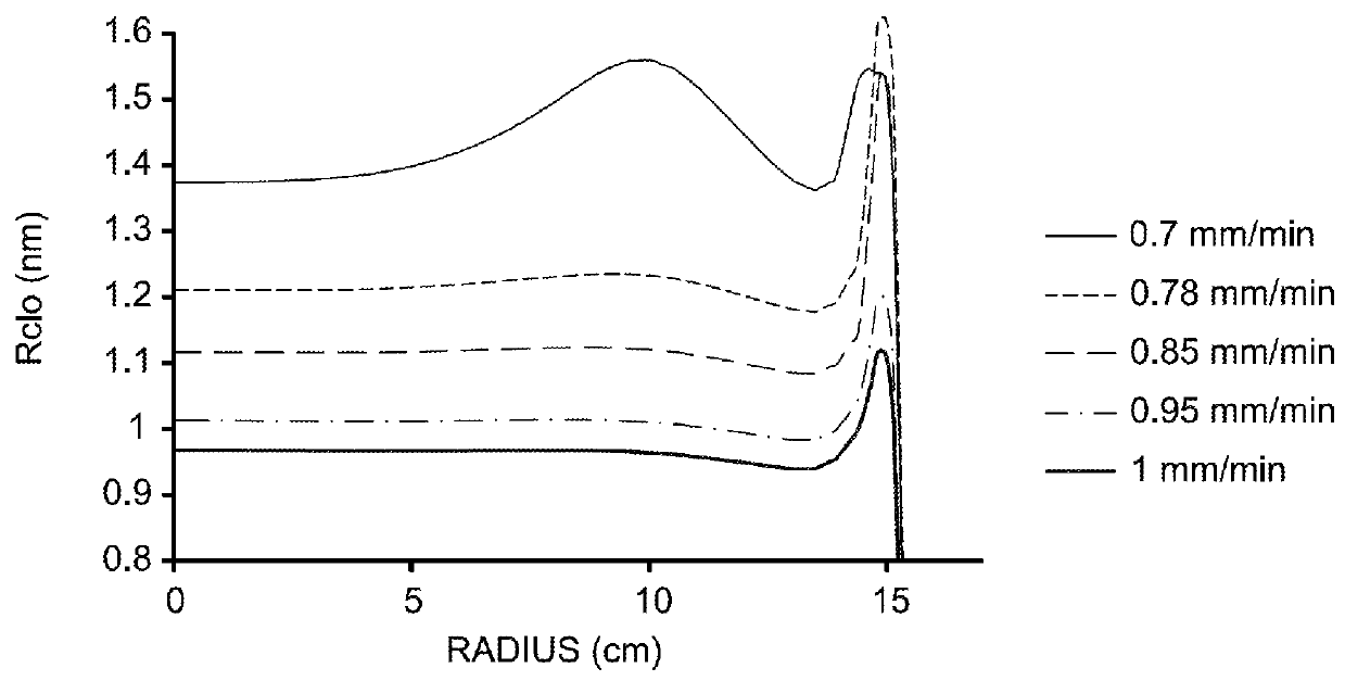
[0101]Simulations were done to derive a set of variables that enable the preparation of 300 mm diameter wafers sliced from nitrogen-doped single crystal silicon ingots wherein the wafers are characterized by substantial radial uniformity of BMD size and distribution. The simulations were based on method depicted in FIG. 23 for the combination of variables disclosed in Table 1 wherein “Comb” refers to combination, “Prior Art” is a comparative prior art ingot. The nitrogen concentration in Table 1 refers to concentration in the silicon melt, wherein the nitrogen concentration in a formed silicon crystal is expected to be in the range of from about 1*1013 atoms per cm3 to about 1*1015 atoms per cm3.

TABLE 1Crystal Surface Pull RateNitrogenTemperatureComb.(mm / min)(atoms / cm3)Gradient (K / cm)Prior Art 0.851.26*101751.1410.91.76*101746.0420.91.26*101746.0430.91.76*101735.8440.91.26*101735.84

[0102]The radii of as-grown oxygen precipitates and radii of as-grown voids at various locations acros...

example 2

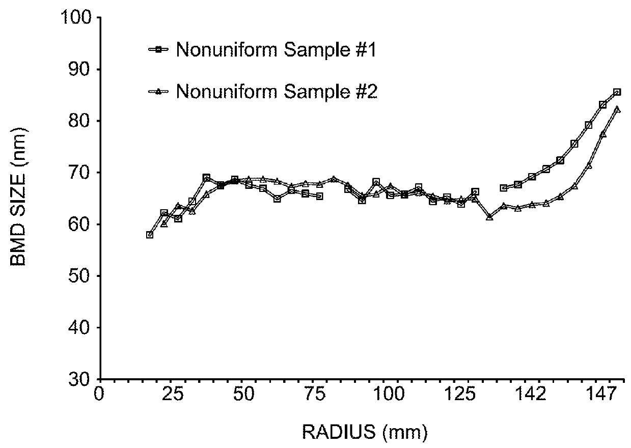
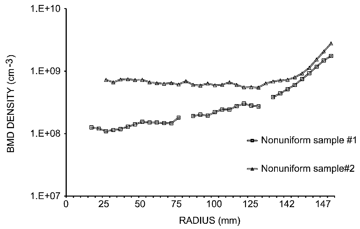
[0104]Three 300 mm diameter single crystal CZ silicon ingots (designated as uniform samples 1, 2 and 3) were each prepared at a pull rate of 0.9 mm per minute, at a temperature gradient of from about 35° K per cm to about 46° K per cm, and at an ingot nitrogen concentration of from about 1*1014 atoms per cubic centimeter to about 1*1015 atoms per cubic centimeter. Comparative 300 mm diameter single crystal CZ silicon ingots (designated as non-uniform samples 1 and 2) were each prepared at a pull rate of 0.78 mm per minute, at a temperature gradient of about 51° K per cm, and at an ingot nitrogen concentration of from about 3*1013 atoms per cubic centimeter to about 2*1014 atoms per cubic centimeter. Wafers were sliced from the ingots and were subjected to an oxygen precipitation heat treatment by annealing the wafer for 3 hours at 780° C. and then 16 hours at 1000° C.

[0105]As depicted in FIG. 1 the average BMD size (diameter) increase from the center of the wafer to the edge of the ...


PUM

PropertyMeasurementUnit
Temperatureaaaaaaaaaa

Abstract

Nitrogen-doped CZ silicon crystal ingots and wafers sliced therefrom are disclosed that provide for post epitaxial thermally treated wafers having oxygen precipitate density and size that are substantially uniformly distributed radially and exhibit the lack of a significant edge effect. Methods for producing such CZ silicon crystal ingots are also provided by controlling the pull rate from molten silicon, the temperature gradient and the nitrogen concentration. Methods for simulating the radial bulk micro defect size distribution, radial bulk micro defect density distribution and oxygen precipitation density distribution of post epitaxial thermally treated wafers sliced from nitrogen-doped CZ silicon crystals are also provided.

Description

CROSS-REFERENCE TO RELATED APPLICATIONS[0001]This application claims priority to U.S. Provisional Application No. 62 / 031,203 filed Jul. 31, 2014.BACKGROUND[0002]The field of the disclosure relates generally to semiconductor grade single crystal silicon which is used in the manufacture of electronic components and methods for preparation thereof. More particularly, the present disclosure relates to vacancy dominated single crystal silicon ingots and wafers sliced therefrom that are doped with nitrogen and provide for thermally treated silicon wafers having oxygen precipitate density and size that are uniformly distributed radially and exhibit the lack of a significant edge effect.[0003]Single crystal silicon, from which a single crystal silicon wafer may be obtained, is commonly prepared by the so-called Czochralski (“CZ”) method. In this method, polycrystalline silicon (“polysilicon”) is charged to a crucible and melted, a seed crystal is brought into contact with the molten silicon...

Claims


Application Information

Patent Timeline
IPC IPC(8): C30B33/02C30B15/04C30B29/06H01L21/02H01L29/167H01L29/32
CPCC30B33/02H01L29/167H01L29/32H01L21/02532C30B29/06H01L21/02694C30B15/04C30B15/203H01L21/02381H01L21/0262H01L21/00C30B15/206
Inventor LU, ZHENGSAMANTA, GAURABLU, TSE-WEITSAI, FENG-CHIEN
Owner GLOBALWAFERS CO LTD
Why Eureka
Try Eureka