Crystalline oxide semiconductor film and semiconductor device
- Summary
- Abstract
- Description
- Claims
- Application Information
AI Technical Summary
Benefits of technology
Problems solved by technology
Method used
Image
Examples
example 2 to example 4
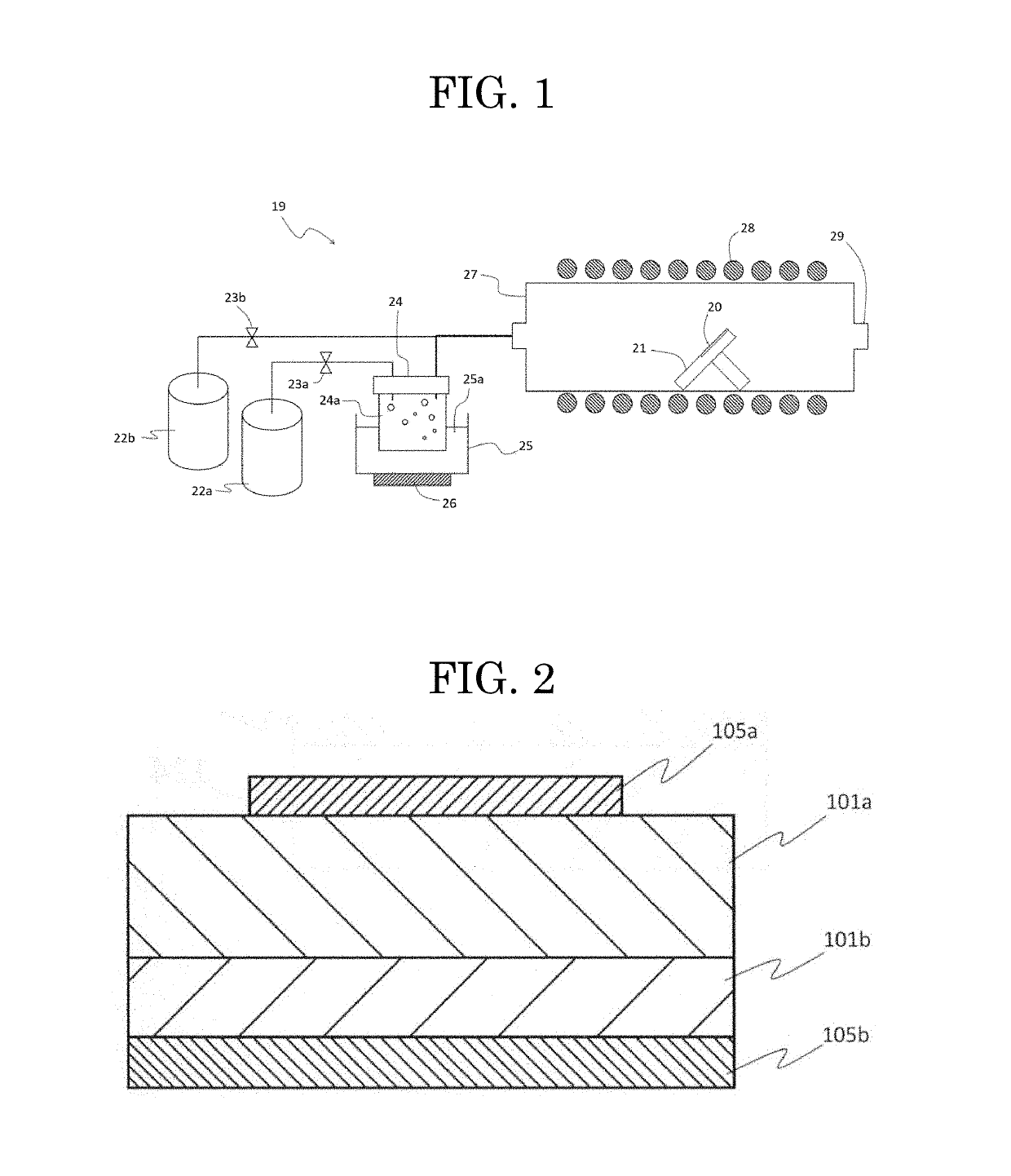
[0074]Crystalline oxide semiconductor films were obtained by the same conditions as the conditions of the Example 1 except the following condition: using an m-plane sapphire substrate with an off-angle as the base. In the Example 2, the off-angle was 0.5°. In the Example 3, the off-angle was 2.0°. In the Example 3, the off-angle was 2.0°. In the Example 4, the off-angle was 3.0°. The crystalline oxide semiconductor film in the Example 2 was 3.0 μm in film thickness. The crystalline oxide semiconductor film in the Example 3 was 2.9 μm in film thickness. The crystalline oxide semiconductor film in the Example 4 was 3.3 μm in film thickness.
example 5
[0075]To confirm reproducibility, a crystalline oxide semiconductor film was obtained by the same conditions as the conditions of the Example 4, and the crystalline oxide semiconductor film obtained herein was 3.4 μm in film thickness. Also, to confirm reproductivity, following Test Examples were conducted, and as clearly shown in Table 1, reproducibility was confirmed to be favorable. Also, the film thickness of the obtained crystalline oxide semiconductor films indicates favorable reproductivity.
example 6
[0076]A crystalline oxide semiconductor film was obtained by the same conditions as the conditions of the Example 1 except the following conditions that gallium bromide and tin bromide are mixed in ultrapure water to be a raw material solution 24a such that the atomic ratio of gallium to tin is 1:0.08 and gallium is 0.1 mol / L in aqueous solution which contains hydrobromic acid that is to be 10% by volume ratio, an a-plane sapphire substrate without a buffer layer on a surface of the a-plane sapphire substrate was used as a base instead of using an m-plane sapphire substrate on that α-Ga2O3 film (non-doped) was arranged as a buffer layer, and the film-formation time was set to be ten minutes.
PUM
| Property | Measurement | Unit |
|---|---|---|
| Angle | aaaaa | aaaaa |
| Angle | aaaaa | aaaaa |
| Area | aaaaa | aaaaa |
Abstract
Description
Claims
Application Information


