Negative electrode active material, negative electrode including the negative electrode active material, secondary battery including the negative electrode, and method of preparing the negative electrode active material
a technology of active materials and negative electrodes, which is applied in the direction of cell components, final product manufacturing, sustainable manufacturing/processing, etc., can solve the problems of process not being simplified and battery cycle characteristics are reduced, and achieve the effect of improving battery cycle characteristics and simplifying the process
- Summary
- Abstract
- Description
- Claims
- Application Information
AI Technical Summary
Benefits of technology
Problems solved by technology
Method used
Image
Examples
example 1
on of Negative Electrode Active Material
[0073](1) Polymer Layer Formation
[0074]The silicon-based compound of Preparation Example 1 was added to a dimethylacetamide (DMAC) solution including poly(acrylic acid) (PAA), and stirred for 1 hour in a reducing atmosphere at room temperature. In this case, Ar gas was used to create the reducing atmosphere. Thereafter, the silicon-based compound was extracted by centrifugation, and a silicon-based compound having PAA coated on the surface thereof was then obtained by vacuum drying. Imidization of the silicon-based compound having PAA coated on the surface thereof was performed by a heat treatment at 300° C. for 60 minutes in a reducing atmosphere of Ar gas, and thus, a 1 μm thick polyimide layer was formed on the silicon-based compound. The thickness of the polyimide layer was measured by transmission electron microscopy.
[0075](2) Formation of Metal Catalyst Layer
[0076]The silicon-based compound having the polyimide layer formed thereon was a...
example 2
on of Negative Electrode Active Material
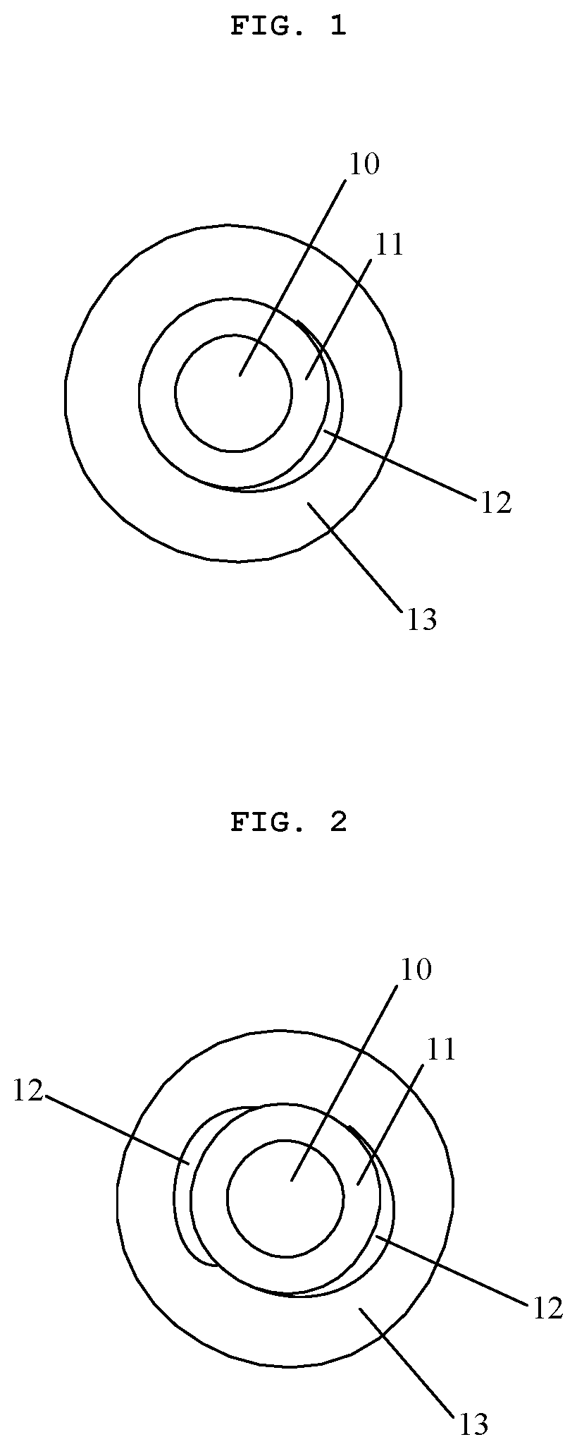
[0081]A negative electrode active material of Example 2 was prepared in the same manner as in Example 1 except that a nickel catalyst layer was formed to a thickness of 50 nm. In the prepared negative electrode active material, the amorphous carbon layer had a thickness of 150 nm, and the graphene layer had a thickness of 25 nm. Also, the at least one cavity had an average thickness in the range of 50 nm or more to less than 100 nm.
examples 3 and 4
and Comparative Examples 4, 5, and 6: Preparation of Secondary Batteries
[0094]Secondary batteries of Examples 3 and 4 and Comparative Examples 4, 5, and 6 were respectively prepared by using the negative electrode active materials of Examples 1 and 2 and Comparative Examples 1, 2, and 3.
[0095]Specifically, each of the negative electrode active materials of Examples 1 and 2 and Comparative Examples 1, 2, and 3, natural graphite, carbon black having an average particle diameter (D50) of 65 nm, CMC, and a styrene-butadiene rubber (SBR) were added and mixed in a weight ratio of 9.6:86.2:1.0:1.7:1.5 with distilled water, as a solvent, to prepare a negative electrode slurry having a solid content of the mixture of 45%.
[0096]Separate 20 μm thick copper (Cu) thin film, as a negative electrode collector, were coated with each negative electrode mixture slurry at a loading amount of 160 mg / 25 cm2 and dried. In this case, a temperature of circulating air was 70° C. Subsequently, each negative ...
PUM
| Property | Measurement | Unit |
|---|---|---|
| thickness | aaaaa | aaaaa |
| thickness | aaaaa | aaaaa |
| temperature | aaaaa | aaaaa |
Abstract
Description
Claims
Application Information

