

High-electron mobility transistor terahertz wave modulator loaded in waveguide
a terahertz wave modulator and high-electron technology, applied in waveguides, waveguide type devices, instruments, etc., can solve the problems of easy interference of external factors, increased difficulty in matching circuits, and increased difficulty in increasing the modulation rate of the modulator, so as to achieve effective control of transmission mode, high modulation efficiency, and high working stability
- Summary
- Abstract
- Description
- Claims
- Application Information
AI Technical Summary
Benefits of technology
Problems solved by technology
Method used
Image

Examples
Embodiment Construction
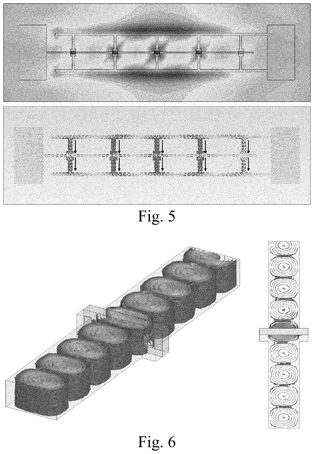
[0032]In the present invention, a modulation chip is prepared by nesting a HEMT in an artificial microstructure, and the modulation chip is loaded into a waveguide cavity, and an external electrical signal is used to change the concentration of 2-DEG in the HEMT, and control the electromagnetic resonance mode in the artificial microstructure Conversion, thereby regulating the transmission of terahertz waves in the waveguide. The simulation calculation shows that it has high modulation efficiency and large modulation depth, and proves that it has extremely high modulation rate in the experiment.
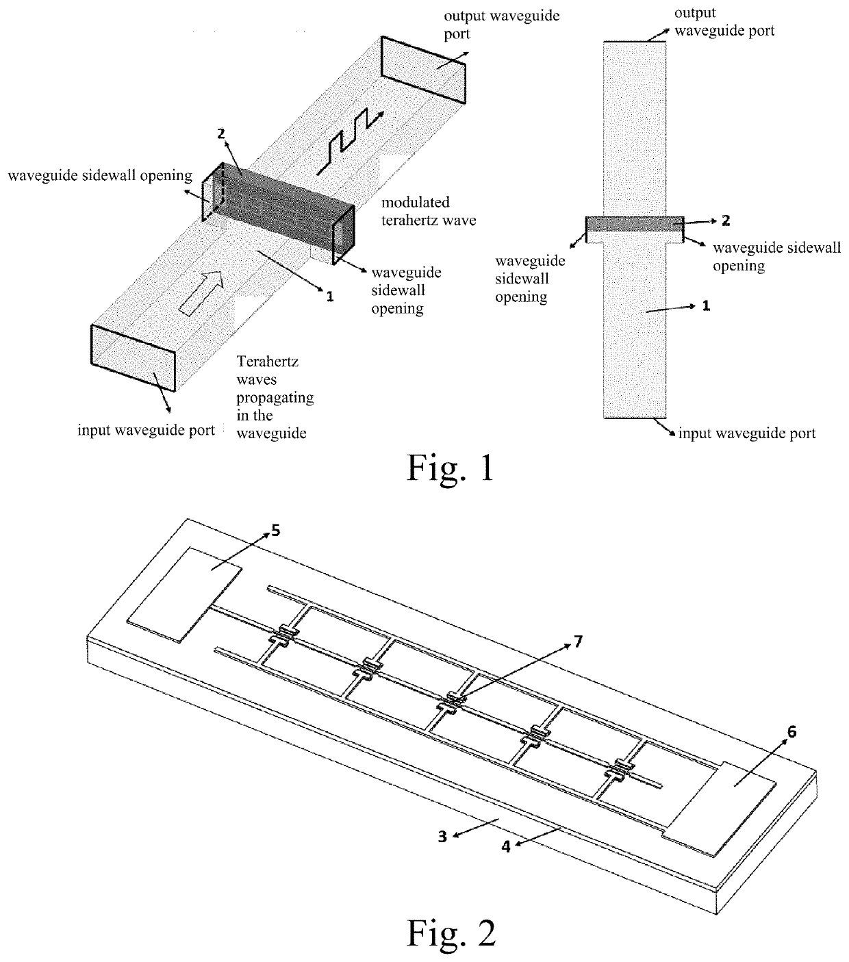
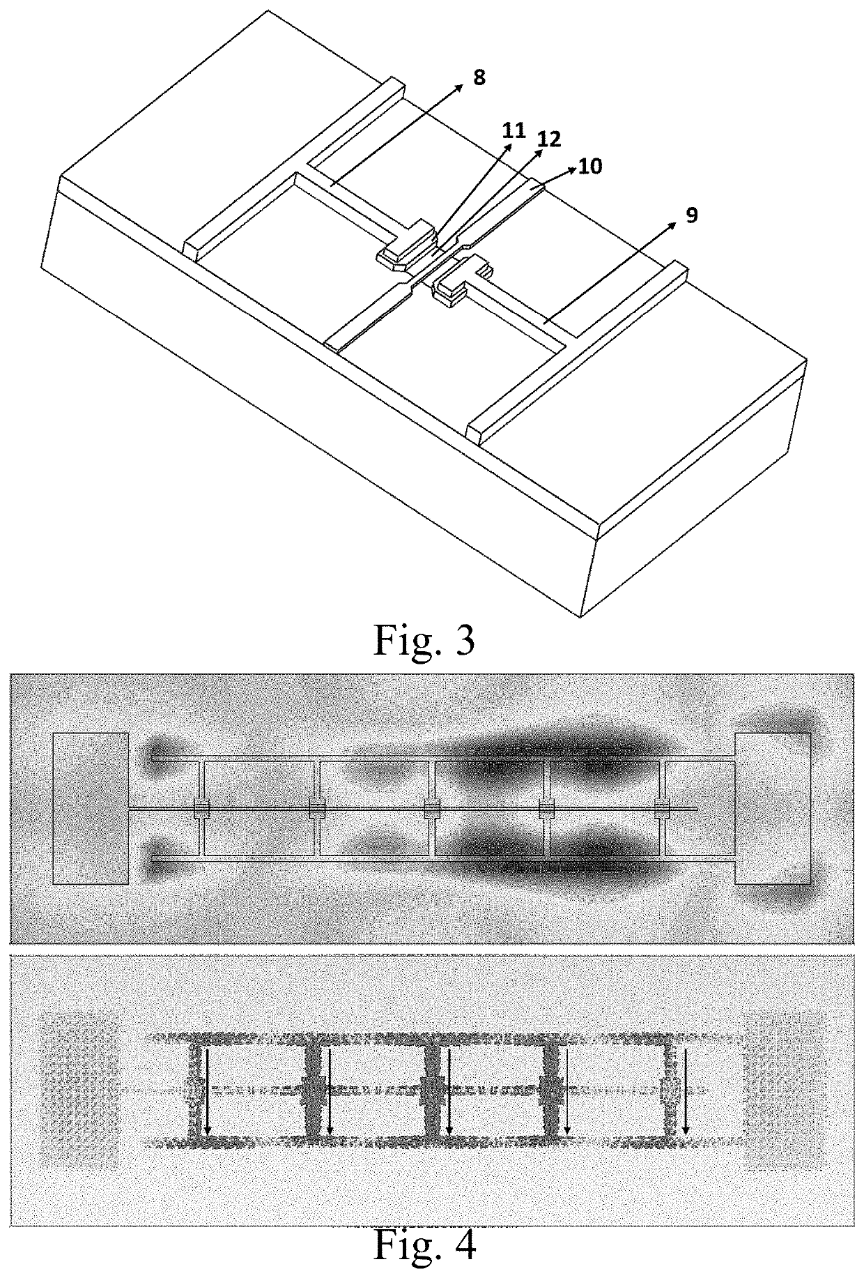
[0033]The invention comprises a rectangular waveguide cavity (1) and a modulation chip (2). The modulation chip (2) includes a semiconductor substrate (3), a heterostructure epitaxial layer (4), a modulation array (7), a positive voltage loading electrode (6), and a negative voltage loading electrode (5). The positive voltage loading electrode (6), the negative voltage loading electrode (5) an...
PUM
| Property | Measurement | Unit |
|---|---|---|
| frequency | aaaaa | aaaaa |
| wavelength | aaaaa | aaaaa |
| wavelength | aaaaa | aaaaa |
Abstract
Description
Claims
Application Information