

Low temperature integrated via and trench fill process and apparatus
a technology of integrated vias and trench filling, which is applied in the direction of vacuum evaporation coatings, basic electric elements, coatings, etc., can solve the problems of defective circuits, voids that are difficult to detect by regular cross sectional standard electron microscopy ("sem
- Summary
- Abstract
- Description
- Claims
- Application Information
AI Technical Summary
Benefits of technology
Problems solved by technology
Method used
Image

Examples
Embodiment Construction
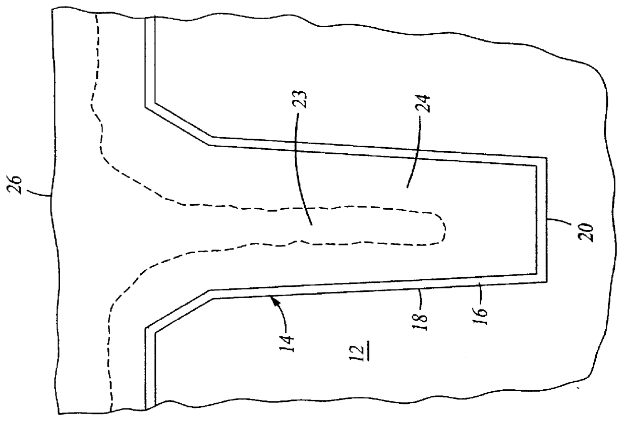
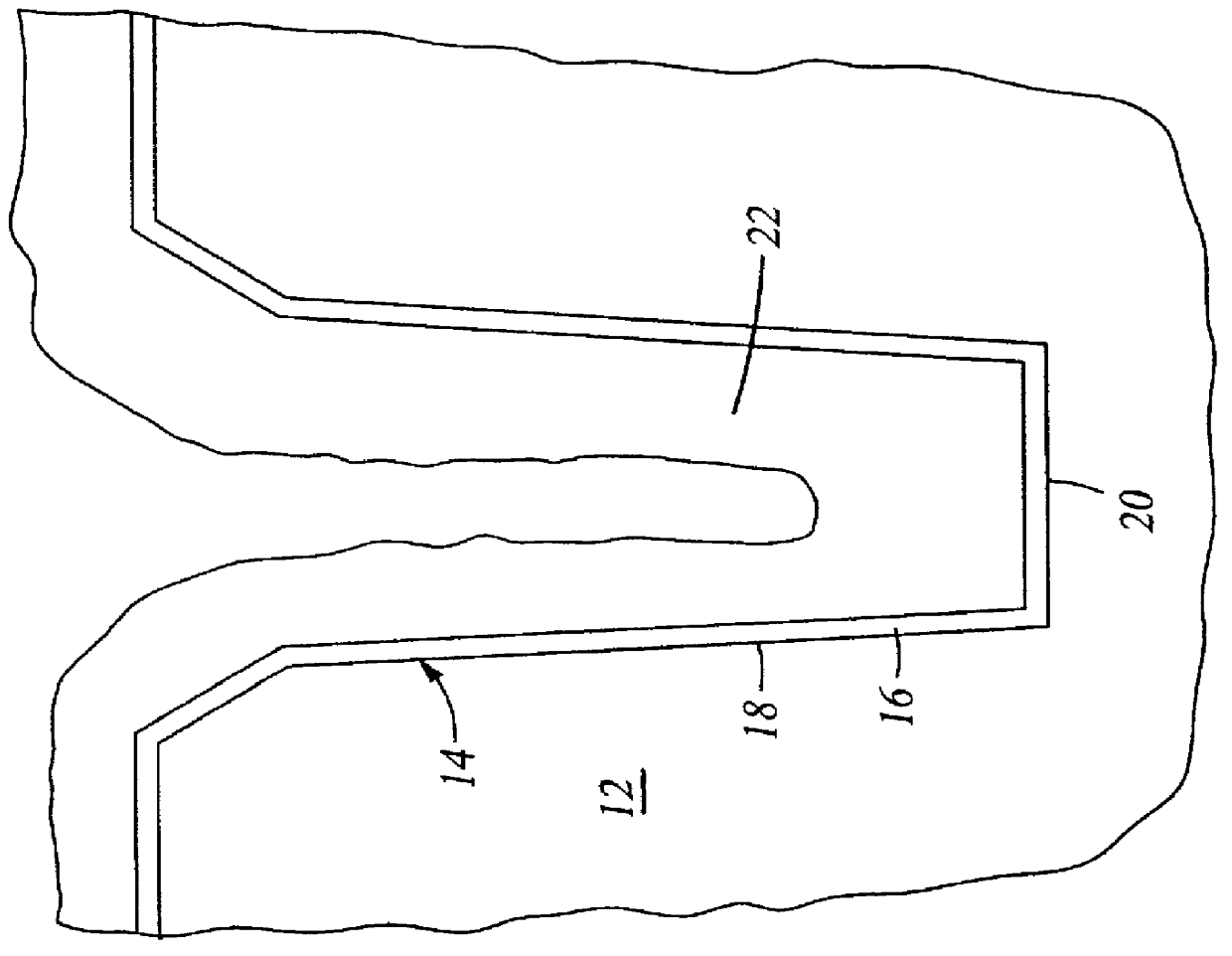
The present invention provides a method for providing improved via fill in high aspect ratio apertures at low temperature, particularly in sub-micron apertures. One aspect of the invention provides a method for metallizing high aspect ratio apertures, including contacts, vias, lines or other features, at temperatures below about 660.degree. C. In particular, the invention provides improved step coverage for filling high aspect ratio apertures in applications with a first layer of a CVD copper ("CVD Cu"), and a second layer of PVD copper ("PVD Cu") where the thin CVD Cu layer is prevented from dewetting on a dielectric layer by capping the dielectric layer with a thin barrier / wetting layer comprised of a refractory metal and / or conductive metal having a melting point greater than that of the CVD Cu and providing greater wetting with the CVD Cu than does the dielectric. A barrier layer, such as tantalum (Ta), is necessary to prevent the diffusion of copper into the adjacent dielectric...
PUM
| Property | Measurement | Unit |
|---|---|---|
| Thickness | aaaaa | aaaaa |
| Thickness | aaaaa | aaaaa |
| Thickness | aaaaa | aaaaa |
Abstract
Description
Claims
Application Information