High power impatt diode

Inactive Publication Date: 2001-06-26
CREE SWEDEN
View PDF11 Cites 7 Cited by
  • Summary
  • Abstract
  • Description
  • Claims
  • Application Information

AI Technical Summary

Problems solved by technology

Such thermal limitations are highly relevant for this type of devices, since the power dissipation is very high, namely more than 50% of the electric power supplied to an IMPATT diode is dissipated within the device as compared to lower frequency power semiconductor switches for which mostly less than 1% of the electric power supplied is dissipated.
However, for different reasons it has until now not been possible to produce any working IMPATT diode of silicon carbide.
The main problem seems to be to take care of the high power dissipated by such a diode.
The high breakdown field of silicon carbide will namely result in such a high breakdown voltage and accordingly operation voltage of the diode that such a diode could not

Method used


Image

  • High power impatt diode
  • High power impatt diode
  • High power impatt diode

Examples


Example

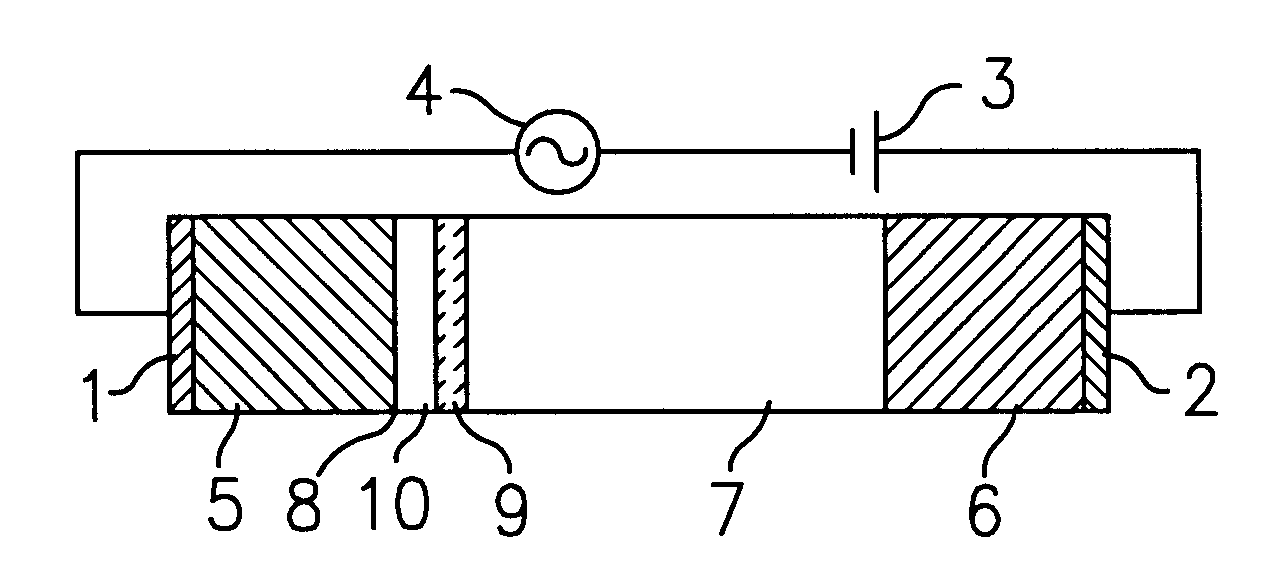
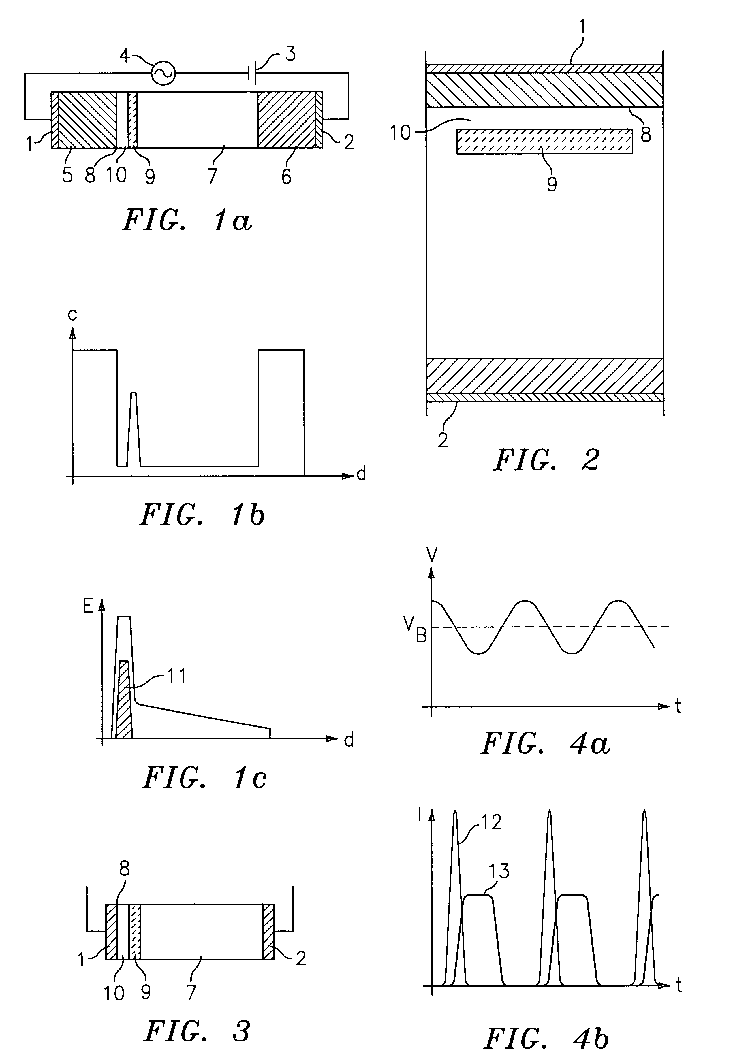
FIG. 1 illustrates a high power IMPATT (Impact Ionisation Avalanche Transit Time) diode for generation of power signals with a frequency above 30 GHz. This diode has two electrodes, namely a cathode 1 and an anode 2, adapted to be connected to a direct voltage source 3 and positioned in a microwave cavity 4 designed so as to have the resonance at desired microwave frequency. A semiconductor layer of crystalline SiC is arranged between the two electrodes and has a highly doped p-type layer 5 in contact with the metal cathode 1, a highly doped n-type layer 6 in contact with the metal anode 2, and a low doped n-type drift layer 7 interconnecting the layers 5 and 6. The layers 5 and 7 forms a pn-junction 8, which is reverse biased by the direct voltage of the direct voltage source 3. Furthermore, a thin n-type layer 9 with a substantially higher doping concentration than the drift layer is arranged in the drift layer 7 at a short distance from the highly doped p-type layer 5. The thin l...


PUM


Abstract

In a high power IMPATT ( Impact Avalanche Transit Time) diode for generating high frequency signals two electrodes, anode (2) and cathode (1), are arranged with a semiconductor layer therebetween. Said semiconductor layer comprises a drift layer (7) for transport of charge carriers between the electrodes. The semiconductor layer is made of crystalline SiC and it is provided with means (9) adapted to locally increase the electric field in the drift layer substantially with respect to the average electric field therein for generating an avalanche breakdown at a considerably lower voltage across the electrodes than would the electric field be substantially constant across the entire drift layer.

Description

FIELD OF THE INVENTION AND PRIOR ARTThe present invention relates to a high power IMPATT (Impact Avalanche Transit Time) diode for generating high frequency signals having two electrodes, an anode and a cathode, and a semiconductor layer therebetween with a junction for blocking conduction of the diode when a voltage is applied in a reverse direction across the electrodes, said semiconductor layer comprising a low doped n-type drift layer between the junction and a first of said electrodes through which charge carriers are transported upon avalanche breakdown in the semiconductor layer and avalanche multiplication of charge carriers when a voltage high enough is applied across the electrodes in said reverse direction.Such a diode employs the avalanche and carrier drift processes occurring in a semiconductor to produce a dynamic negative resistance at microwave frequencies. This diode is one of the most powerful sources of microwave power. It may be used to produce high power signals...

Claims


Application Information

Patent Timeline
IPC IPC(8): H01L29/66H01L29/864H01L29/02H01L29/24
CPCH01L29/864H01L29/1608
Inventor HARRIS, CHRISTOPHERKONSTANTINOV, ANDREI
Owner CREE SWEDEN
Why Eureka
Try Eureka