Organic electroluminescent device

an electroluminescent device and organic technology, applied in the direction of discharge tube/lamp details, discharge tube luminescnet screens, organic semiconductor devices, etc., can solve the problems of high cost, high cost, and high cost of devices, and achieve the effect of maintenance, reducing the cost of production, and improving the reliability of devices

Inactive Publication Date: 2001-11-13
FUTABA CORPORATION
View PDF19 Cites 42 Cited by
  • Summary
  • Abstract
  • Description
  • Claims
  • Application Information

AI Technical Summary

Problems solved by technology

A problem common to these organic EL devices is reliability.
However, these materials are sensitive to damage during device fabrication, and offer a problem in conjunction with an affinity for electrodes.
Another problem is that the deterioration of an organic thin film is much severer than that of an LED or LD.
Most organic materials are relatively expensive.
However, it is still difficult to obtain an organic EL device superior to prior art organic ELs in terms of emission performance and basic device reliability.

Method used


Image

  • Organic electroluminescent device
  • Organic electroluminescent device
  • Organic electroluminescent device

Examples


example 1

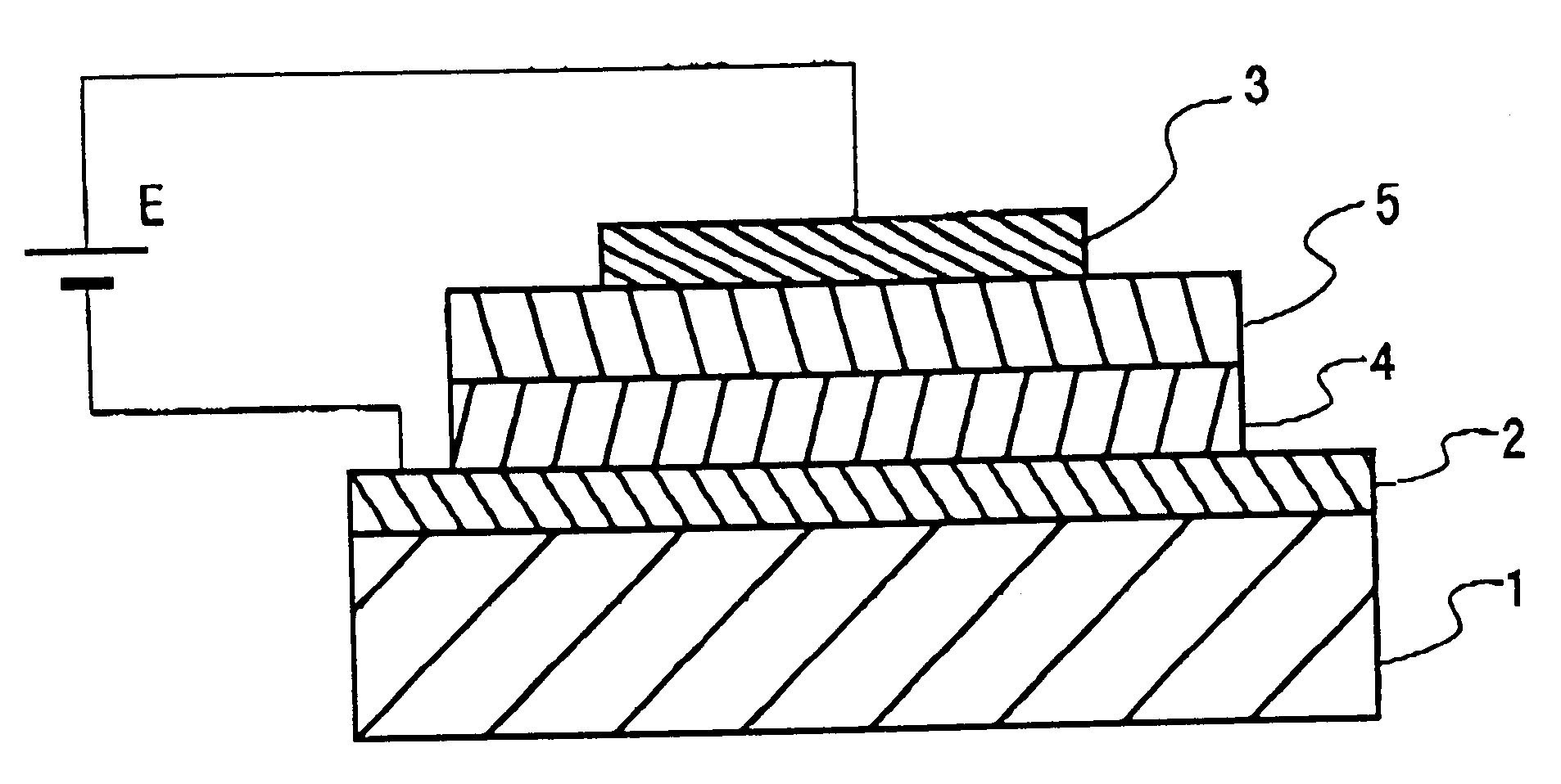
A 7059 substrate (made by Corning) used as a glass substrate was scrubbed with neutral detergent.

Then, the substrate was fixed to a substrate holder in a vacuum evaporation system, which was evacuated to a vacuum of 1.times.10.sup.-4 Pa or lower. With the vacuum kept, Al was deposited by evaporation to a thickness of 200 nm thereby forming a cathode.

With the vacuum still kept, the substrate with the cathode formed thereon was transferred into a sputtering system where an inorganic insulating electron injecting layer was formed to a thickness of 1 nm, using as a target a mixture of strontium oxide (SrO) and 25 mol % of hafnium oxide (HfO.sub.2). Regarding the film formation conditions applied to this end, the substrate temperature was 25.degree. C., a mixture of Ar and O.sub.2 at 1:1 was used for the sputtering gas, the film formation rate was 1 nm / min., the operating pressure was 0.5 Pa, and the input power was 5 W / cm.sup.2.

With the vacuum still kept, N, N, N', N'-tetrakis(m-bipheny...
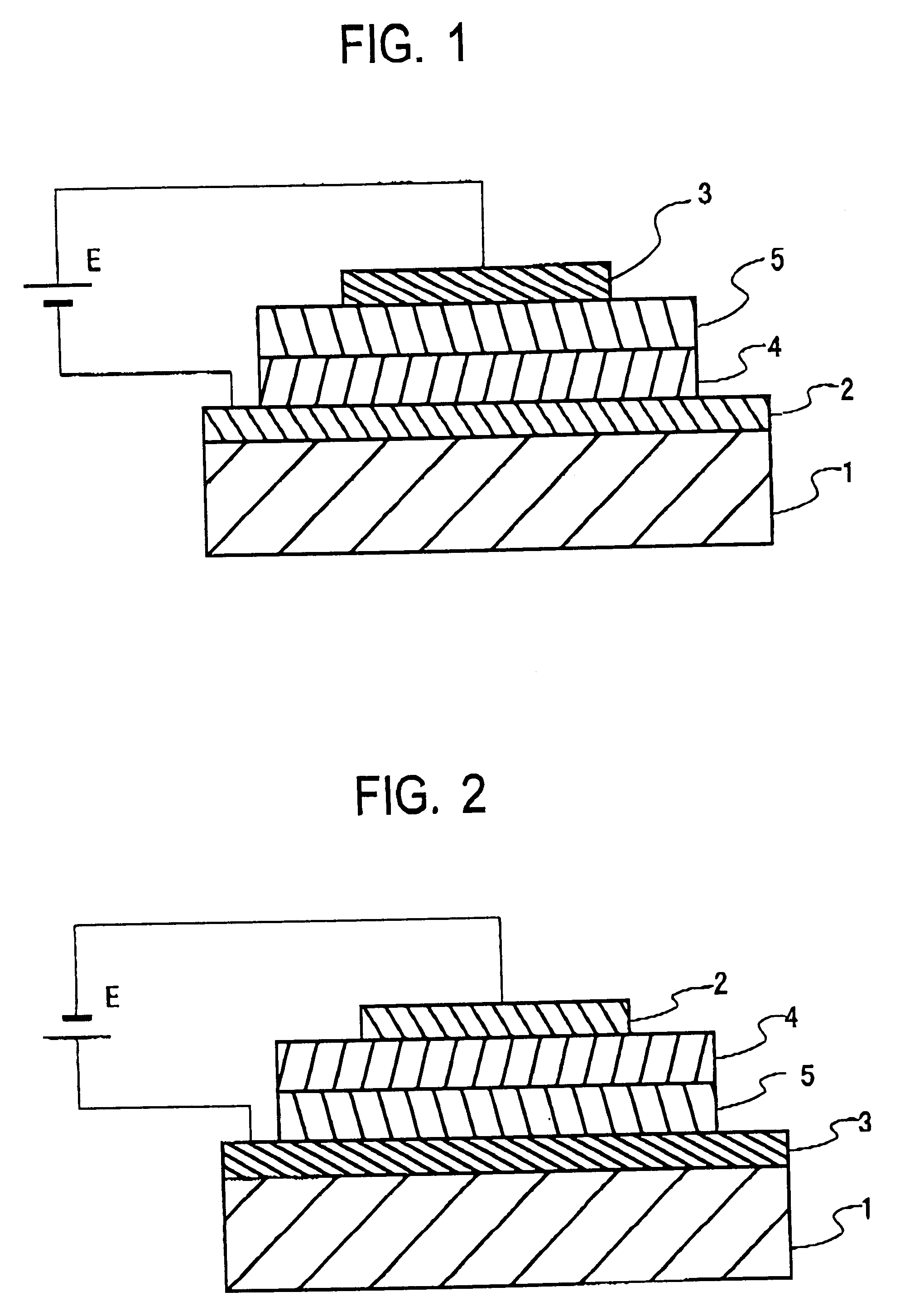
example 2

An organic EL device was prepared as in Example 1 with the exception that the inorganic insulating electron injecting layer was formed using strontium oxide (SrO) as the oxide having a low work function and cerium oxide (Ce.sub.2 O.sub.3) as the oxide having a high work function.

When this organic EL device was continuously driven with a constant current of 100 mA / cm.sup.2 as in Example 1, the initial luminance was equivalent to that of Example 1. Even after the passage of 300 hours, at least 80% of the initial luminance was still kept. In the organic EL device of this example, neither current leakage nor dark spots were observed.

example 3

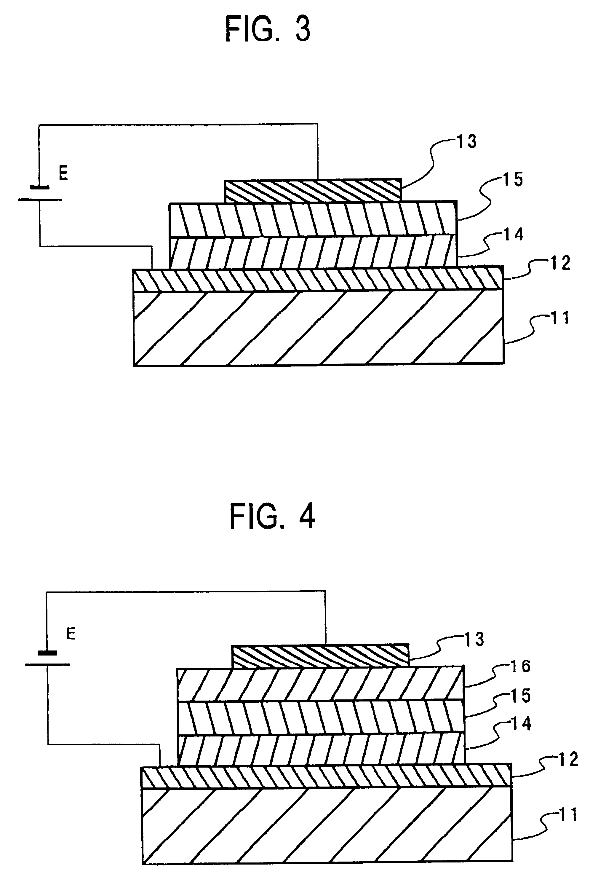
Organic EL devices were prepared as in Example 1 with the exception that electron injecting layers were formed using as the oxide having a low work function lithium oxide (Li.sub.2 O), sodium oxide (Na.sub.2 O), potassium oxide (K.sub.2 O), rubidium oxide (Rb.sub.2 O), cesium oxide (Cs.sub.2 O), calcium oxide (CaO), barium oxide (BaO), and yttrium oxide (Y.sub.2 O.sub.3) instead of strontium oxide (SrO). The same effect as in Example 1 was obtained.

Organic EL devices were prepared as in Example 1. Instead of hafnium oxide (HfO.sub.2), however, beryllium oxide (BeO), magnesium oxide (MgO), titanium oxide (TiO, TiO.sub.2), iron oxide (FeO), zirconium oxide (ZrO.sub.2), lanthanum oxide (La.sub.2 O.sub.3), praseodymium oxide (Pr.sub.2 O.sub.3), neodymium oxide (Nd.sub.2 O.sub.3), samarium oxide (Sm.sub.2 O.sub.3), europium oxide (Eu.sub.2 O.sub.3), gadolinium oxide (Gd.sub.2 O.sub.3), terbium oxide (Tb.sub.2 O.sub.3), dysprosium oxide (Dy.sub.2 O.sub.3), holmium oxide (Ho.sub.2 O.sub.3)...


PUM


Abstract

The object of the invention is to provide an organic EL device which possesses the merits of both an organic material and an inorganic material, has an extended life, an improved efficiency, a low driving voltage and high luminance, and is fabricated at low cost. This object is achieved by the provision of an organic EL device comprising a substrate, a hole injecting electrode and a cathode formed on the substrate, and at least one organic layer located between these electrodes. An inorganic insulating electron injecting layer is located between the cathode and the organic layer. The inorganic insulating electron injecting layer comprises as an oxide having a low work function at least one oxide having a work function of lower than 2.5 eV, and as an oxide having a high work function at one oxide having a work function of 2.5 to 4 eV.

Description

BACKGROUND OF THE INVENTION TECHNICAL ARTThe present invention relates generally to an organic EL (electroluminescent) device, and more specifically to an inorganic / organic junction structure used for a device comprising an organic compound thin film which emits light at an applied electric field.In general, an organic EL device is basically built up of an ITO or other transparent electrode formed on a glass substrate, an organic amine base hole transporting layer laminated on the transparent electrode, an organic light emitting layer formed of a material having electronic conductivity and giving out strong light emission, for instance, an Alq.sup.3 material, and an electrode provided on the organic light emitting layer and formed of a material having a low work function, for instance, an MgAg material.As reported so far in the art, the device has a structure wherein one or plural organic compound layers are interleaved between a hole injecting electrode and an electron injecting el...

Claims


Application Information

Patent Timeline
Patent Type & Authority Patents(United States)
IPC IPC(8): H01L51/50H01L51/52H05B33/12H05B33/14H05B33/22
CPCH01L51/5092H01L2251/5346H10K50/171H10K2101/80
Inventor ARAI, MICHIOKOBORI, ISAMUMITSUHASHI, ETSUO
Owner FUTABA CORPORATION
Why Eureka
Try Eureka