Stencil reticle incorporating scattering features for electron beam projection lithography

a technology of electron beam and scattering features, applied in the field of charged particle beam optical systems, can solve the problems of increasing the cost of production of even modest numbers of moderately complex integrated circuit designs, and affecting the quality of electron beam projection lithography

Inactive Publication Date: 2003-04-01
NIKON CORP
View PDF2 Cites 7 Cited by
  • Summary
  • Abstract
  • Description
  • Claims
  • Application Information

AI Technical Summary

Problems solved by technology

As chip complexity has increased, the throughput of such tools has become generally prohibitive for production of even modest numbers of a moderately complex integrated circuit design of high integration density.
At the same time, however, problems in projection fidelity and image quality not previously recognized or considered to be of practical importance have become critical to high manufacturing yields of high integration density chips, particularly as minimum feature size has been extended into regimes below one-tenth micron.
Many of these problems are inherent in the electron beam optics in regard to proper abutment of sub-fields and aberrations which may be difficult to avoid.
Other problems accrue from the complex dynamics of the beam of charged particles, itself, and the interaction of the beam with a target and / or the reticle.
These backscattered electrons will also cause exposure of the resist.
In broad areas of resist to be exposed, the additional over-exposure will be of little practical effect when the backscattering occurs into regions which are also exposed.
The complexity and magnitude of the effect and corresponding exposure artifacts are increased in charged particle beam projection systems because of the relatively large area (e.g. 1 / 4 mm to 1 mm square) sub-field exposure area and the complexity of the pattern therein.
The net effect is one of local defocussing the beam and variation of the focal plane with percentage of exposed area in the pattern, causing variable blurring of portions of the image.
This type of mask is not generally favored since the high degree of absorption of charged particles and corresponding current causes heating and mask distortion.
Therefore, efforts to compensate for the proximity effect such as edge or feature size adjustment (by "trimming" of the reticle features), multiple exposures (e.g. illuminating the reticle with differently patterned beams), "ghost" corrections (using scattered electrons to provide background dose boost), dose modulation (standard in probe-forming systems but inapplicable to projection systems) and the like greatly increase complexity of the exposure process and potentially compromise the success of the process because they inherently involve the accuracy of respective portions of the reticle, may not be controllable enough at a local level, reduce system throughput and / or require registration of plural exposures.
Compensation for local Coulomb effect would require regulation of percentage area of exposure in the circuit design which is not at all practical and, even if possible, would unacceptably constrain integrated circuit layout designers.

Method used


Image

  • Stencil reticle incorporating scattering features for electron beam projection lithography
  • Stencil reticle incorporating scattering features for electron beam projection lithography
  • Stencil reticle incorporating scattering features for electron beam projection lithography

Examples


Embodiment Construction

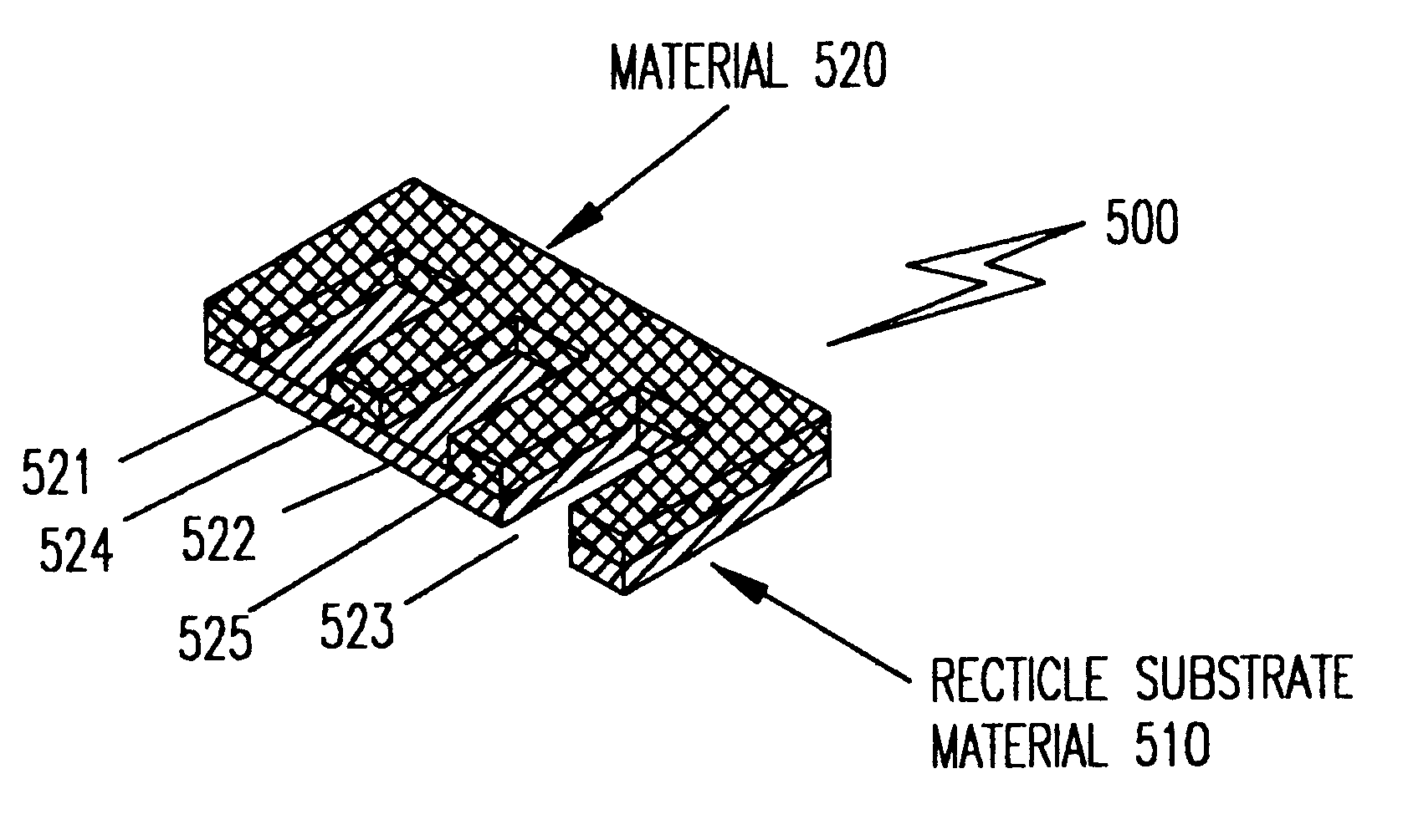
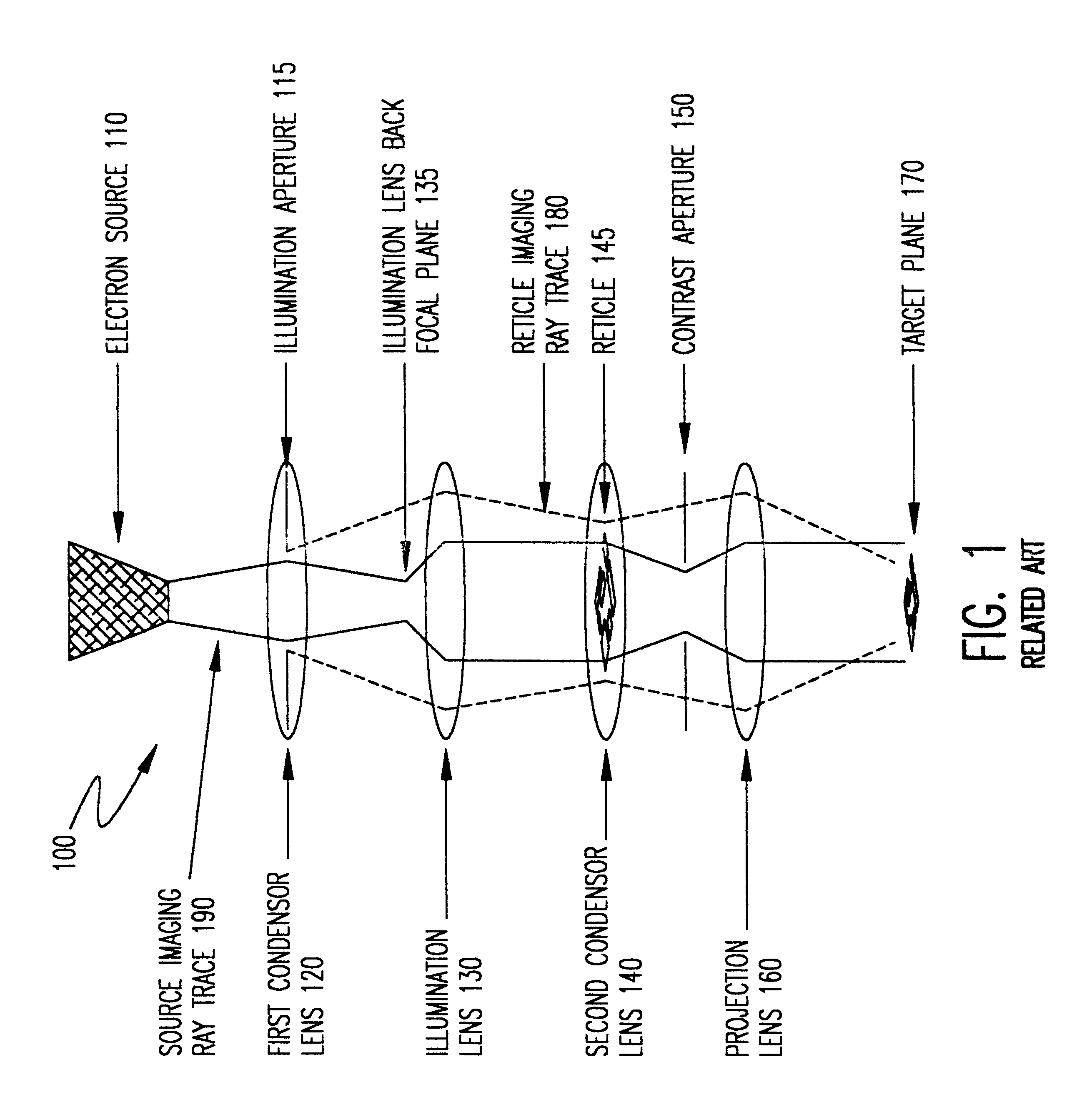
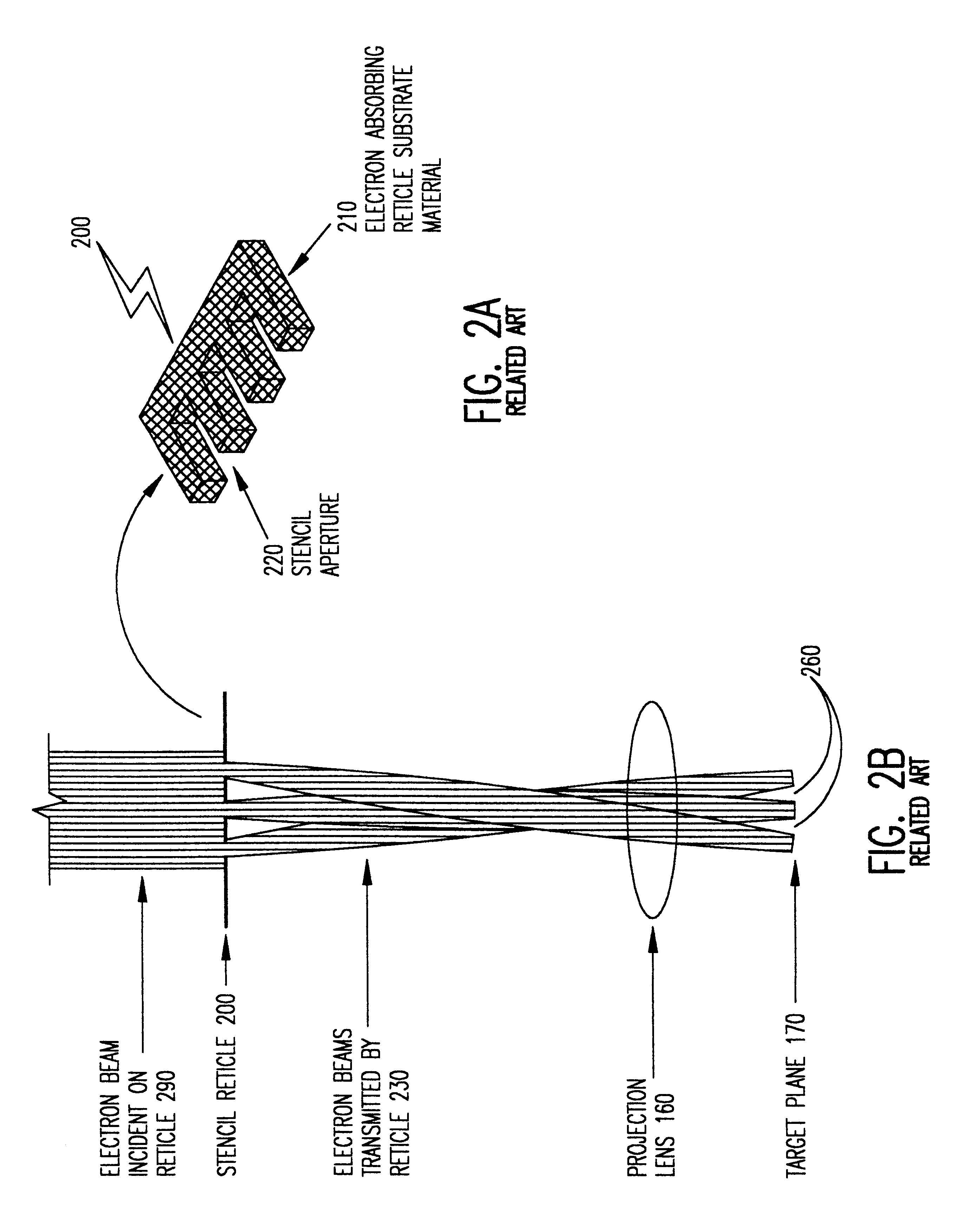
Referring now to the drawings, and more particularly to FIG. 1, there is shown, in highly schematic and much simplified form, the major elements of an electron beam projection system 100. In FIG. 1, as in other Figures, structures and functions are depicted in a manner considered most useful in conveying an understanding of the invention. The term "known" is used to refer to that over which the present invention provides an improvement but is specifically not intended as an admission of prior art in regard to the present invention. It should also be understood that the basic principles of the invention are grounded in the enhancement and exploitation of a combination of effects largely unrecognized and unexploited, even singly, in known reticles and which are best explained in connection with structures considered "known". Accordingly, FIGS. 1-4B are denoted as "Related Art" in order to accurately reflect their connection with and relevance to the present invention, including the as...


PUM

PropertyMeasurementUnit
atomic numberaaaaaaaaaa
thicknessaaaaaaaaaa
densityaaaaaaaaaa

Abstract

Proximity (exposure dose) effects and/or local Coulomb (space charge defocussing) effects, both dependent on local pattern density of exposed areas, are simultaneously compensated in a charged particle beam projection device or tool by a projection reticle having an apertured weakly scattering membrane with selective strongly scattering regions between the apertures in the membrane. A reticle so constructed provides at least three independent exposure dosage levels that can be mixed to provide a wide range of exposure levels with high contrast. The more weakly the electrons are scattered (in the extreme, the electrons are not scattered at all through apertures), the greater the number that pass through a given beam contrast aperture, the higher the corresponding dose received at the target plane and the more space charge is contained in the beam bundle. Therefore, to compensate for the proximity effect (i.e. provide dose boost) and the local Coulomb effect (i.e. provide additional space charge) regions with reduced scattering characteristics are employed. Use of a hybrid doped resist allows exposure corresponding to an intermediate exposure dose in a preferred variant implementation exploiting the three dosage levels developed.

Description

1. Field of the InventionThe present invention generally relates to charged particle beam optical systems and, more particularly, to enhancement of exposures made by projection of a reticle pattern onto a target.2. Description of the Prior ArtNumerous lithography techniques are known and are in widespread use for manufacture of integrated circuit devices, in particular. Essentially, such lithography processes define potentially very minute areas and shapes on a surface through selective exposure and removal of portions of a layer of resist to expose areas of the surface for further processing by, for example, etching, implantation and / or deposition. Exposure has generally been accomplished in the past by use of radiant energy such as visible wavelength light.There is a strong incentive in the manufacture of integrated circuits to increase integration density to the greatest possible degree consistent with acceptable manufacturing yields. Device arrays of increased density provide in...

Claims


Application Information

Patent Timeline
Patent Type & Authority Patents(United States)
IPC IPC(8): G03F1/16H01J37/317G03F1/20G03F7/20H01L21/027
CPCB82Y10/00B82Y40/00H01J37/3174G03F1/20H01J2237/31794
Inventor ROBINSON, CHRISTOPHER F.STICKEL, WERNER
Owner NIKON CORP
Why Eureka
Try Eureka