Method for preparing epitaxial-substrate and method for manufacturing semiconductor device employing the same

a gallium nitride and compound semiconductor technology, applied in the direction of polycrystalline material growth, crystal growth process, after-treatment details, etc., can solve the problems of poor surface morphology, many irregularities on the surface, and poor surface morphology

Inactive Publication Date: 2003-09-30
KK TOSHIBA
View PDF21 Cites 137 Cited by
  • Summary
  • Abstract
  • Description
  • Claims
  • Application Information

AI Technical Summary

Problems solved by technology

The surface of, for example, a GaN layer grown directly on a sapphire (Al.sub.2 O.sub.3) substrate by the MOCVD method has faults and the surface morphology is very poor due to the formation of hexagonal pyramid-like or hexagonal shaped patterns resulting in numerous irregularities on the surface.
Manufacturing of semiconductor device such as a blue light emitting diode (hereafter referred as "the LED") using the semiconductor crystalline layer having very poor surface morphology such that the numerous irregularities are present is practically impossible due to very low yield.
However, the method described above is required to control very small quantity of feed gas, because the growing condition of buffer layer is limited strictly and further, because the film thickness must be controlled very accurately and strictly.
However, when gallium chloride (GaCl) formed by supplying hydrogen chloride (HCl) gas so as to contact with liquid gallium is used, the control range of feed quantity is much higher than that for the case of using MO gas, so that the control performance and the reproducibility are extremely low.
However, it is difficult to improve crystal quality and surface morphology of a laminated structure of the GaN based semiconductor formed on the thick single crystalline GaN based semiconductor layer grown by this method.
Furthermore, the crystal quality and the surface morphology are not sufficiently good to fabricate a practical semiconductor laser diode, so that a noticeable improvement of the crystal quality is required.
Especially, it is well known that the existence of large crystal defect called "nanopipe" is a large problem in an improvement of semiconductor device particularly in reliability.
In the conventional light emitting device using a single crystalline GaN based semiconductor layer, because the sapphire substrate popularly employed for the epitaxial growth was insulating, it was not possible to dispose the electrode layer on the back surface.
In particular, since the GaN based semiconductor is a material difficult to etch, the formation of trench for forming the electrode is difficult and the fabrication processes are complicated.
As the region of the trench for disposing the electrode occupied a certain area, the entire size could not be made small and so the yield was low.
Such a difficulty was a serious problem especially in integrated structures.
Though the GaN bulk substrate, or the substrate obtained from the bulk single crystal of GaN, may be the ideal substrate for an epitaxial growth of a single crystalline GaN based semiconductor layer, an excellent GaN bulk substrate is not commercially available, because an excellent single crystal of the GaN, or GaN based semiconductor has not yet been obtained in the state of art.
Thickness more than 500 .mu.m of the epitaxial-substrate may be unpractical because of the longer growing time resulting in the lower productivity, although it may possible to obtain the thicker epitaxial-substrate.
Furthermore, the direct ohmic contact of a metal electrode to the back surface of the epitaxial-substrate obviates the necessity of the etching process for forming the electrode, and only single wire bonding is needed for one light emitting device.

Method used


Image

  • Method for preparing epitaxial-substrate and method for manufacturing semiconductor device employing the same
  • Method for preparing epitaxial-substrate and method for manufacturing semiconductor device employing the same
  • Method for preparing epitaxial-substrate and method for manufacturing semiconductor device employing the same

Examples


first embodiment

acturing LD

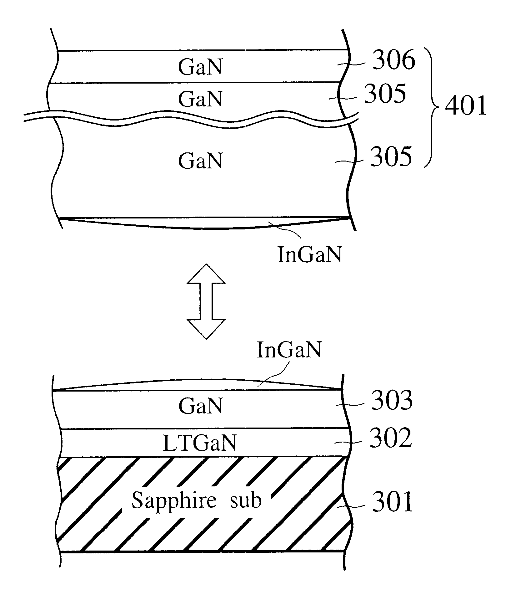
Next, as an example of the method for manufacturing the semiconductor device according to first embodiment of the present invention using the GaN epitaxial-substrate 401 thus obtained, a method of fabricating a blue-emitting LD will be described.

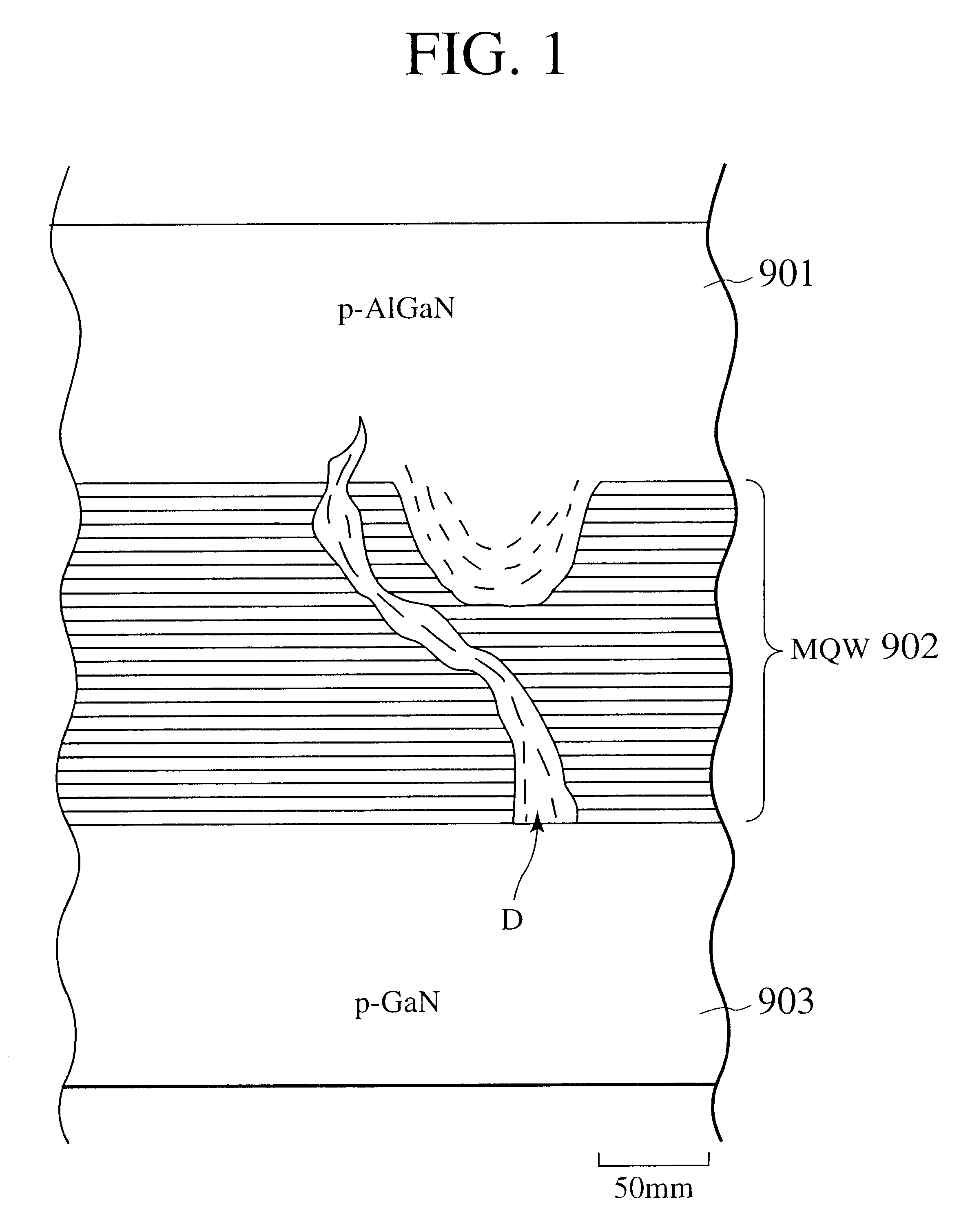
First, a device structure of the blue-emitting LD, which is an object of the method of manufacturing the semiconductor device according to the first embodiment, will be briefly described. The blue-emitting LD is based on a structure wherein an n-GaN epitaxial layer 402, an n-AlGaN epitaxial layer 403, an n-GaN epitaxial layer 404, an MQW active layer 405, a p-AlGaN epitaxial layer 406, a p-GaN epitaxial layer 407, a p-AlGaN epitaxial layer 408, a p-GaN epitaxial layer 409, an n-GaN epitaxial layer 410, a p 4GaN epitaxial layer 51, a p-GaN epitaxi al layer 52 are stacked in this order on the GaN epitaxial-substrate 401 as shown in FIG. 6A. As shown in FIG. 6D, a concave region through the n-GaN epitaxial layer 410, reaching to the ...

first modification

of First Embodiment

Next, a method for manufacturing a semiconductor device according to a modification (first modification) of the first embodiment using the AlGaN / GaN epitaxial-substrate 411 shown in FIG. 4D will be described referring to FIGS. 7A and 7B. The blue-emitting LD according to the first modification of the first embodiment shown in FIG. 7B can be fabricated by the processes similar to the process sequence shown in FIGS. 6A to 6D.

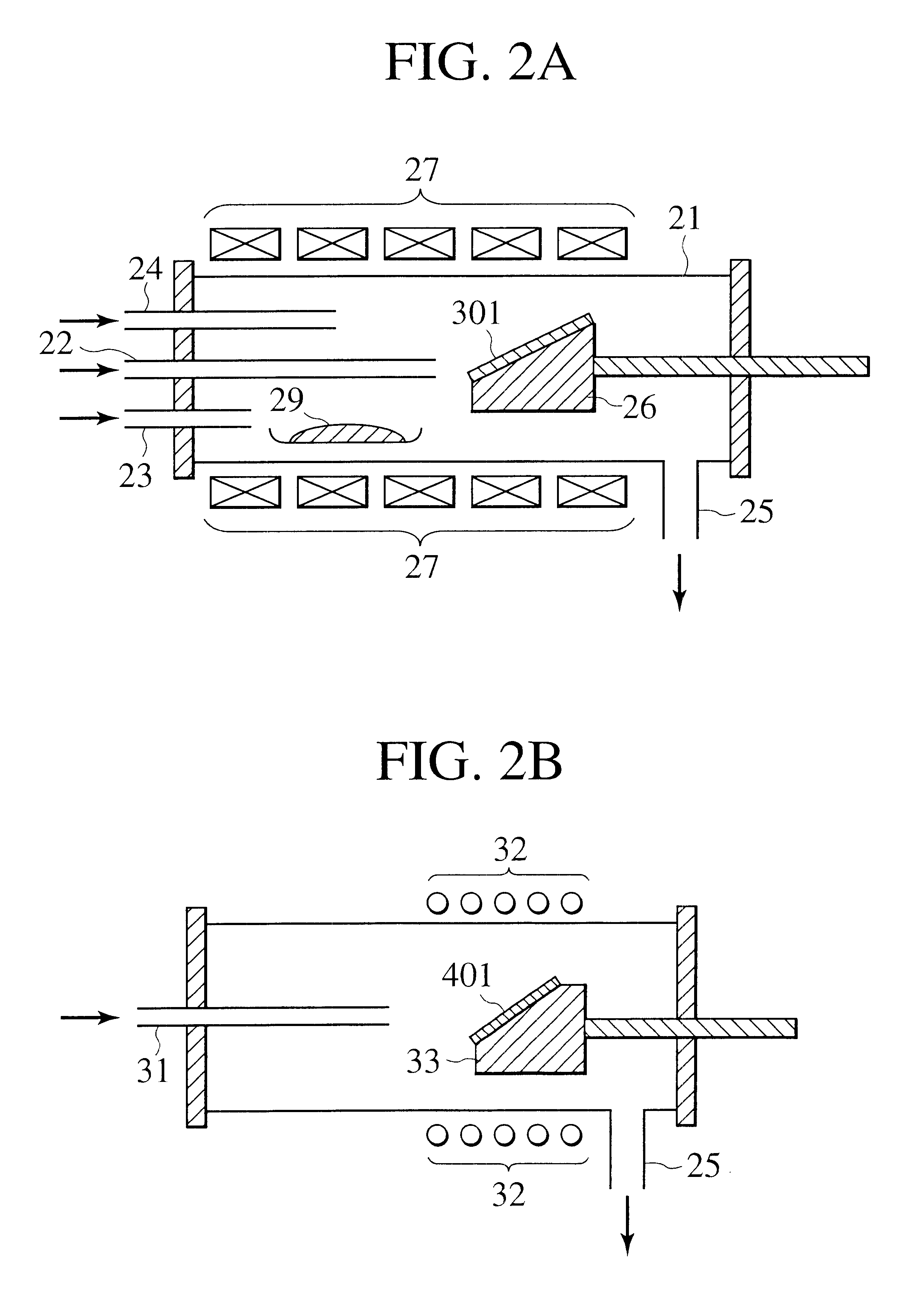
(a) First, the AlGaN / GaN epitaxial-substrate 411 located on a susceptor 33 is heated by RF power radiated from the RF heater 32, while supplying hydrogen, nitrogen and NH.sub.3 gases from a gas introduction tube 31 of the MOCVD equipment shown in FIG. 2B and then the susceptor temperature is controlled to be 1150.degree. C. Next, supply of TMG and SiH.sub.4 gases diluted by hydrogen gas is started and a Si-doped n-GaN epitaxial layer 402 is grown to a thickness of 4 .mu.m on the AlGaN / GaN epitaxial-substrate 411. Thereafter, a Si-doped n-AlGaN e...

second modification

of First Embodiment

Next, a method for manufacturing a semiconductor device according to a modification (second modification) of the first embodiment using the AlGaN epitaxial-substrate 421 shown in FIG. 5B will be described referring to FIGS. 8A and 8B. The blue-emitting LD according to the second modification of the first embodiment shown in FIG. 8B can be fabricated by the processes similar to the process sequence shown in FIGS. 6A to 6D.

(a) First, the AlGaN epitaxial-substrate 421 located on a susceptor 33 is heated by RF power radiated from the RF heater 32, while supplying hydrogen, nitrogen and NH.sub.3 gases from a gas introduction tube 31 of the MOCVD equipment shown in FIG. 2B and then the susceptor temperature is controlled to be 1150.degree. C. Next, supply of TMG gas and SiH.sub.4 diluted by hydrogen gas is a started and an n-GaN epitaxial layer 402 is grown on the AlGaN epitaxial-substrate 421. Thereafter, an n-AlGaN epitaxial layer 403 is grown on the n-GaN epitaxial l...


PUM

PropertyMeasurementUnit
thicknessaaaaaaaaaa
thicknessaaaaaaaaaa
thicknessaaaaaaaaaa

Abstract

The present invention provides a method for preparing epitaxial-substrate, for growing a multilayered structure of GaN based semiconductor layers on the epitaxial-substrate so as to construct a semiconductor device such as blue-emitting laser diode and LED. The method for preparing the epitaxial-substrate encompasses (a) growing a first GaN based semiconductor layer on a bulk-substrate; (b) growing an InGaN based semiconductor layer on the first GaN based semiconductor layer; (c) growing a second GaN based semiconductor layer on the InGaN based semiconductor layer; and (d) separating the second GaN based semiconductor layer from the first GaN based semiconductor layer to provide the epitaxial-substrate. The epitaxial-substrate having a high crystallographic perfection and an excellent surface morphology is obtained simply and in a short time. The defect density of the single crystalline GaN based semiconductor layer film grown on the epitaxial-substrate is greatly reduced.

Description

1. Field of the InventionThe present invention pertains to a vapor phase epitaxial growth technology of a single crystalline gallium nitride (GaN) based compound semiconductor, more particularly to a method of fabricating a single crystalline substrate (wafer) of GaN based compound semiconductor (hereinafter referred as "the GaN based semiconductor") having an excellent crystallographic quality and to a method of manufacturing a semiconductor device using this single crystalline wafer of GaN based semiconductor.2. Description of the Related ArtRecently, blue light emitting semiconductor devices and electronic devices using a single crystalline GaN based semiconductor as a material are attracting attention. A metalorganic compound chemical vapor deposition method (hereafter referred as "the MOCVD method") is well known as a method of growing crystalline GaN based semiconductor. The MOCVD method is one of the epitaxial growth methods with which a single crystalline compound semiconduc...

Claims


Application Information

Patent Timeline
Patent Type & Authority Patents(United States)
IPC IPC(8): H01L21/02H01L21/205H01L33/00C30B29/38C30B25/18H01L33/32
CPCH01L21/0242H01L21/02458H01L21/02502H01L21/02505H01L21/0254H01L21/02573H01L21/0262H01L21/02664H01L33/007
Inventor NISHIO, JOHJIISHIKAWA, MASAYUKI
Owner KK TOSHIBA
Why Eureka
Try Eureka