Semiconductor device with tapered gate and insulating film

a technology of insulating film and tapered gate, which is applied in the direction of optics, transistors, instruments, etc., can solve the problems of increasing the number of process steps, the inability to use the tapered gate to form a driver circuit for performing image display, and the complexity of the manufacturing process

Inactive Publication Date: 2003-11-11
SEMICON ENERGY LAB CO LTD
View PDF41 Cites 208 Cited by
  • Summary
  • Abstract
  • Description
  • Claims
  • Application Information

AI Technical Summary

Problems solved by technology

Therefore, even though they can be used as switching elements for driving a liquid crystal in the pixel portion in an active matrix type liquid crystal display device (switching elements formed by TFTs are hereafter referred to as pixel TFTs), it is impossible to use them to form a driver circuit for performing image display.
Forming the active layer by a crystalline semiconductor layer is superior when comparing TFT characteristics, but there are problems in that the manufacturing process becomes complex, and the number of process steps increases, in order to manufacture a TFT corresponding to each circuit in addition to the pixel TFT.
It is clear that the increase in the number of process steps is a cause of inc

Method used


Image

  • Semiconductor device with tapered gate and insulating film
  • Semiconductor device with tapered gate and insulating film
  • Semiconductor device with tapered gate and insulating film

Examples


embodiment 1

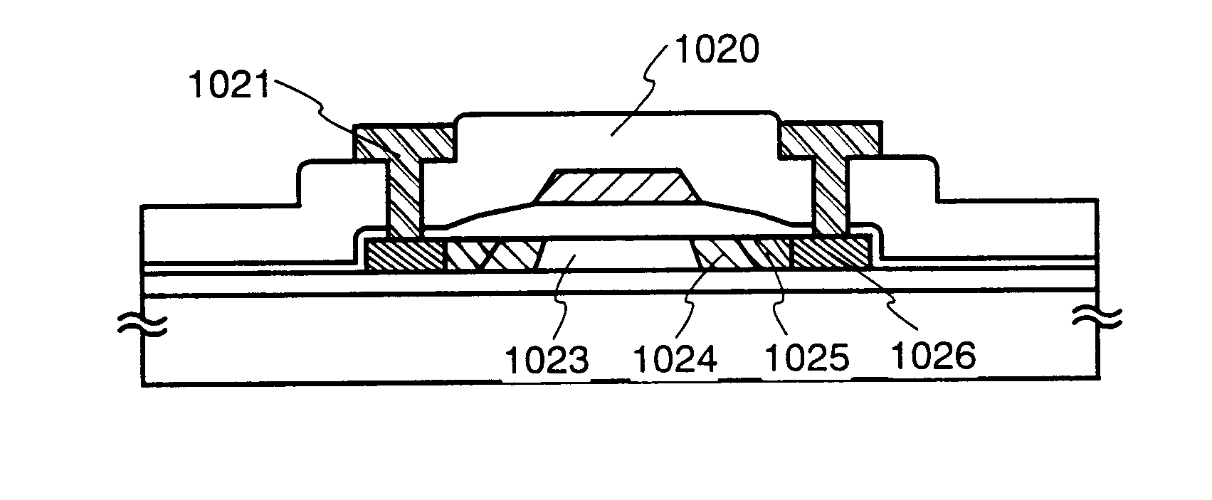
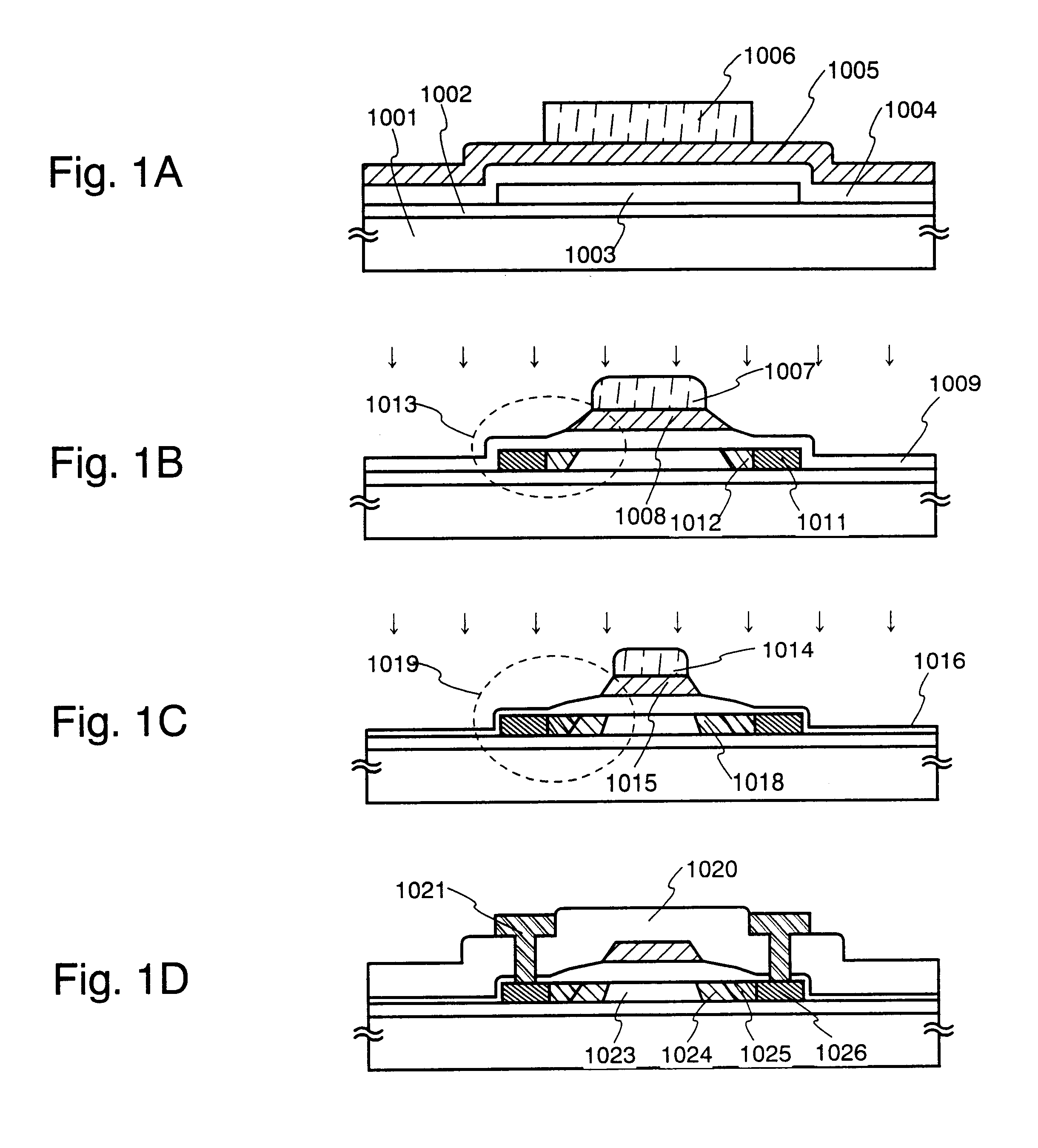
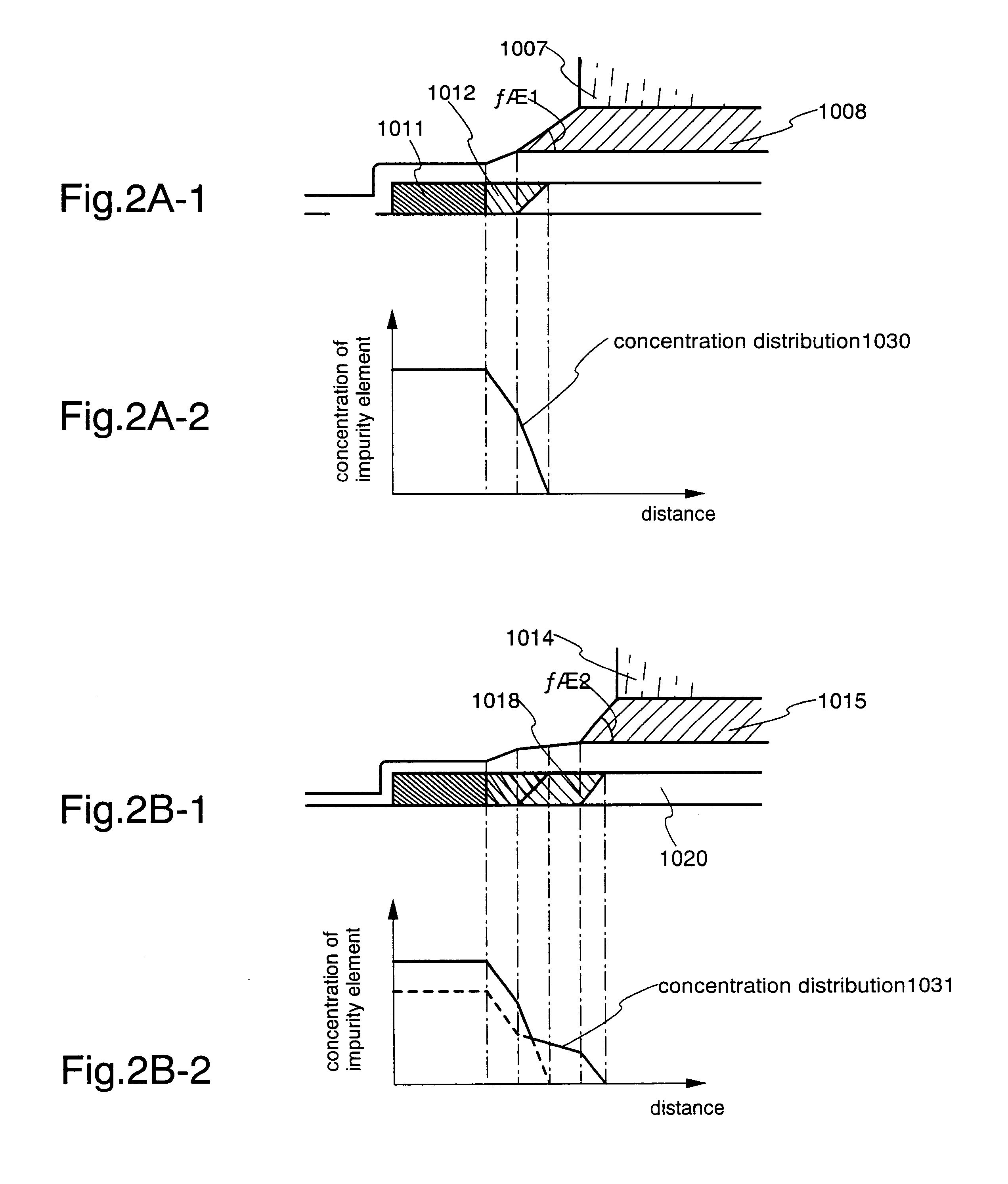
An Embodiment of the present invention is explained using FIGS. 3A to 5B. A method of manufacturing a pixel TFT and a storage capacitor of a pixel portion, and a driver circuit TFT formed in the periphery of the pixel portion, at the same time is explained in detail here in accordance with process steps.

In FIG. 3A, a glass substrate such as barium borosilicate glass or aluminum borosilicate glass, typically Corning Corp. #7059 or #1737 glass, or a quartz substrate is used as a substrate 101. When using a glass substrate, heat treatment may be performed in advance at a temperature between 10 and 20.degree. C. below the distortion temperature of the glass. A base film 102 is then formed from an insulating film such as a silicon oxide film, a silicon nitride film, or a silicon nitride oxide film on the surface of the substrate 101 on which a TFT will be formed, in order to prevent impurity element diffusion. For example, a lamination of a silicon nitride oxide film 102a having a thickn...

embodiment 2

Examples of using heat-resistant conductive materials such as W and Ta as materials for the gate electrode were shown in Embodiment 1. The reason for using these materials resides in that it is necessary to activate the impurity element that was doped into the semiconductor layer for the purpose of controlling the conductive type after the formation of the gate electrode by thermal annealing at between 400.degree. C. and 700.degree. C. By implementing this step, it is necessary that the gate electrode has heat-resistivity. However, this type of heat-resistant conductive material has a sheet resistivity of about 10 W, and hence is not always suitable for a display device having a screen size of a 4-inch class or more. This is because if a gate wiring to be connected to the gate electrode is formed of the same material, then the length of the lead wiring on the substrate inevitably becomes large. Thus, the problem of a wiring delay caused by the influence of wiring resistance cannot b...

embodiment 3

The active matrix substrate manufactured in Embodiment 1 is applicable for a reflection type display device as it is. On the other hand, in the case of applying it to a transmission type liquid crystal display device, it is appropriate to form the pixel electrodes provided in each pixel of the pixel portion with transparent electrodes. A method of manufacturing an active matrix substrate corresponding to the transmission type liquid crystal display device is explained in Embodiment 3 with references to FIG. 10.

The active matrix substrate is manufactured in the same way as Embodiment 1. In FIG. 10A, a conductive metallic film is formed by sputtering or vacuum evaporation to form a source wiring and a drain wiring. This structure will be explained in detail with reference to FIG. 10B using the drain wiring 256 as an example. A Ti film 256a is formed at a thickness of between 50 and 150 nm, and then a contact is formed with a semiconductor film that forms the source or the drain region...


PUM


Abstract

In a semiconductor device, typically an active matrix display device, the structure of TFTs arranged in the respective circuits are made suitable in accordance with the function of the circuit, and along with improving the operating characteristics and the reliability of the semiconductor device, the manufacturing cost is reduced and the yield is increased by reducing the number of process steps. A semiconductor device has a semiconductor layer, an insulating film formed contacting the semiconductor layer, and a gate electrode having a tapered portion on the insulating film, in the semiconductor device, the semiconductor layer has a channel forming region, a first impurity region for forming a source region or a drain region and containing a single conductivity type impurity element, and a second impurity region for forming an LDD region contacting the channel forming region, a portion of the second impurity region is formed overlapping a gate electrode, and the concentration of the single conductivity type impurity element contained in the second impurity region becomes larger with distance from the channel forming region.

Description

1. Field of the InventionThe present invention relates to a semiconductor device having a circuit structured by a thin film transistor (hereafter referred to as a TFT) on a substrate having an insulating surface, and to a method of manufacture thereof. In particular, the present invention provides an electro-optical device, typically a liquid crystal display device or an EL display device in which a pixel portion and a driver circuit are formed on the same substrate, and provides a technique of suitably utilizing this type of electro-optical device loaded into electronic equipment. Note that, throughout this specification, the term semiconductor device indicates a general device functioning by utilizing semiconductor characteristics, and the above electro-optical device, and equipment in which the electro-optical device is loaded, are included in the category of semiconductor device.2. Description of the Related ArtA display device structured by a pixel portion in which active eleme...

Claims


Application Information

Patent Timeline
IPC IPC(8): H01L21/70H01L29/786H01L21/02H01L27/12H01L21/336H01L21/84H01L29/66H01L29/40H01L29/423H01L21/77
CPCH01L29/42384H01L27/1214H01L29/66757H01L29/78621H01L29/78627H01L33/62H01L33/08H01L29/4908H01L27/12H01L27/124H01L27/127H01L2924/0002H01L2029/7863H01L2924/00G02F1/13624H01L27/1222
Inventor ONO, KOJISUZAWA, HIDEOMIARAO, TATSUYA
Owner SEMICON ENERGY LAB CO LTD
Why Eureka
Try Eureka