Light emitting device

a technology of light-emitting devices and light-emitting layers, which is applied in the direction of thermoelectric devices, electroluminescent light sources, electric lighting sources, etc., can solve the problems of inhibiting current flow, difficult to form fluorescence conversion layers and/or color filter layers on organic el structures in desired patterns, and degrading electrode materials and thin films such as el films

Inactive Publication Date: 2004-08-24
FUTABA CORPORATION
View PDF11 Cites 68 Cited by
  • Summary
  • Abstract
  • Description
  • Claims
  • Application Information

AI Technical Summary

Problems solved by technology

When highly heat resistant films such as polyimide and aramid films are used as the flexible base material, there may arise a problem that since these films are hydrophilic, outgassing due to water or moisture absorption of the films causes degradation of electrode materials and thin films such as EL film.
However, to form the fluorescence conversion layer and / or the color filter layers on the organic EL structure in a desired pattern is very difficult from the standpoints of patterning technique and damages to the organic EL structure.
In an alternative wherein the fluorescence conversion layer and / or the color filter layers are formed on a substrate in a desired pattern and the organic EL structure is laid thereon, steps resulting from the patterning cause breaks or discontinuities of the overlying film or disconnection of wiring strips, which inhibits current flow with a failure to operate as an organic EL device.
Another problem is that moisture and gases emanating from the fluorescence conversion layer and / or the color filter layers can damage organic layers and electrodes and corrode the electrodes.
This approach yet leaves unsolved the problem that moisture and gases can damage organic layers and electrodes and corrode the electrodes.
These attempts are impractical for some reason or other that the moisture or gas impermeable effect of the film is insufficient, the surface flatness thereof is problematic, and the fluorescence conversion layer and / or the color filter layer or the overcoat layer serving as the underlying layer can be damaged by the conditions during formation of the passivation film.
However, a thick passivation film takes a long time to deposit and is poorly productive.
An additional problem is that the film produced by the dry process has considerable internal stresses so that it may be readily cracked, failing to exert the passivation effect.
In general, as the resin base material becomes thinner, its surface protecting effect becomes weaker.
Inversely, if the resin base material is as thick as about 500 to 1,000 .mu.m, there is a tendency for flexibility and light transmittance to decline.
In contrast, too thin a film fails to fulfil the insulation required as a protective film or color filter overcoating film or the function as a heat resistant, surface leveling passivation film whereas too thick a film is likely to sacrifice flexibility in the application where flexibility is required.
As the organic solvent, alcohol solvents which readily react with polysilazane are undesired.
The photo-polymerization initiator contributes little to conversion of inorganic polysilazane to silica and excessive amounts thereof detract from the denseness of converted silica film.
If the transmittance is low, the silica film tends to attenuate the light emission from the light emitting layer, failing to reach the luminance level necessary as the light emitting device.
With a lower transmittance, the light emitted by the light emitting layer is attenuated through the electrode, failing to provide a luminance necessary as a light emitting device.
Although the upper limit of the electrode thickness is not critical, a too thick electrode would cause a drop of transmittance and separation.
Too thin an electrode is insufficient for its effect and low in film strength during fabrication.
While the thickness of the light-emitting layer is not critical, it is appreciated that too large a thickness results in an increased drive voltage whereas too small a thickness leads to a drop of light emission efficiency.

Method used


Image

  • Light emitting device
  • Light emitting device
  • Light emitting device

Examples


example 1-1

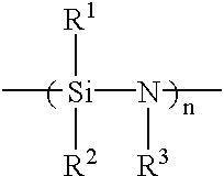
A polyether sulfone resin sheet of 200 .mu.m thick, which is colorless, transparent as demonstrated by an overall light transmittance of at least 90% and heat resistant as demonstrated by a Tg of 230.degree. C. (FS-5300 by Sumitomo Bakelite Co., Ltd.) was used as a base material 1 as shown in FIG. 1. This substrate 1 on both surfaces was coated with a 20 wt % dibutyl ether (DBE) solution of partially methyl-modified polysilazane (10 at % of hydrogen in the structure being substituted) (L710 by Tonen Corp., Pd catalyst-containing product) by dip coating, and dried by heating. While supplying humid air (humidified by bubbling air into pure water) into a clean oven held at 200.degree. C., the coated substrate was subjected to steam oxidation by heating in the oven for 2 hours. The coated substrate was then heat treated in an air atmosphere at 230.degree. C. for one hour. There was obtained a flexible transparent substrate having a dense silica layer of about 1.2 .mu.m thick containing ...

example 1-2

A 7059 glass substrate (Corning Glass Works) as a base material, after cleaning, was immersed in a 0.3% aqueous solution of KBM603 (Shin-Etsu Silicone Co., Ltd.), washed with water, treated with a silane coupling agent, and baked at 220.degree. C. for one hour.

Then, a red Transer film (Fuji Photo Film Co., Ltd.) was laminated to the substrate at 130.degree. C., a pressure of 2 MPa and a rate of 1.4 m / min. Then the base film of the Transer film was stripped. After masking with a red mask, the film was entirely exposed to a ultrahigh pressure mercury lamp so as to give an integral dose of 50 to 100 mJ / cm.sup.2.

Next, red pixels were formed by a process using a selected developer and developing agent. Using the ultrahigh pressure mercury lamp, post-exposure was carried out from both the back surface of the glass substrate and the pixel-forming surface and to an exposure dose of 500 mJ / cm.sup.2. The glass substrate was further baked at 220.degree. C. for 120 minutes, obtaining a color fi...

example 1-3

An alumina substrate was used as a substrate 11 as shown in FIG. 2. On the substrate 11, an Al electrode 12 was formed to a thickness of 200 nm by an RF sputtering technique. Next, by an RF sputtering technique using a target containing SiO.sub.2, BaO, B.sub.2 O.sub.3, Al.sub.2 O.sub.3 and CaO in a weight ratio of 45:30:12:12:1 under conditions: input power 1.5 kW, O.sub.2 2% and 0.4 Pa, the material was deposited to a thickness of 100 nm. This was annealed at 220.degree. C. for 4 hours for crystallization, obtaining a lower insulating layer 13 in the form of a glass ceramic film.

On the lower insulating layer, a ZnS:Mn phosphor thin film (light emitting layer) 14 of 600 nm thick was formed at a substrate temperature of 200.degree. C. by an EB evaporation technique and annealed in vacuum at 600.degree. C. for 10 minutes. Then, a SrS:Ce phosphor thin film 14 of 600 nm thick was formed at a substrate temperature of 550.degree. C. by an RF magnetron sputtering technique using Ar gas and...


PUM


Abstract

The invention aims to provide a light emitting device comprising a base material or protective member which has improved light transmittance, heat resistance, passivation (gas barrier, oligomer release prevention and minimized outgassing), anti-water or moisture-absorption, stability against chemical degradation, dimensional and shape stability, anti-surface-reflection, electrical insulation, UV degradation resistance, and weather resistance, and is highly productive due to possible film formation under atmospheric pressure, and hence, a light emitting device featuring high reliability, ease of manufacture and low cost. The object is attained by a light emitting device comprising a base material (1) having flexibility, light transparency and heat resistance, a lower electrode (4) having light transmittance, a light emitting layer (4), and an upper electrode (4) formed on the base material, the device further comprising a silica film and/or a siliceous film (3) which is formed on the substrate side as viewed from the light emitting layer (4) or on opposite sides of the substrate by applying polysilazane and subjecting it to oxidative treatment.

Description

1. Field of the InventionThis invention relates to light emitting devices comprising a base material or protective member having flexibility, light transmittance, weather resistance, heat resistance and electrical insulation as well as improved passivation, and more particularly, to organic EL devices using the same.2. Description of the BackgroundOrganic EL devices have a basic configuration including a hole injecting electrode of tin-doped indium oxide (ITO) etc., a hole transporting material such as triphenyldiamine deposited thereon, a light emitting layer of a fluorescent material such as aluminum quinolinol complex (Alq3) stacked thereon, and an electrode (electron injecting electrode) of a metal having a low work function such as Mg. The devices produce a very high luminance of several 100 to several 10,000 cd / m.sup.2 when driven at a voltage of about 10 volts.For the application of such organic EL devices to portable equipment, flexible materials such as resin film are of in...

Claims


Application Information

Patent Timeline
Patent Type & Authority Patents(United States)
IPC IPC(8): H01L27/32H01L51/50H01L27/28H01L51/52H05B33/10H05B33/04
CPCH01L51/5253H05B33/04H05B33/10H01L27/3244H01L51/529H10K59/12H10K50/87H10K50/844
Inventor KUBOTA, YUICHIARAI, MICHIO
Owner FUTABA CORPORATION
Why Eureka
Try Eureka