Semiconductor device formed over a surface with a depression portion and a projection portion
Inactive Publication Date: 2005-01-11
SEMICON ENERGY LAB CO LTD
View PDF4 Cites 65 Cited by
Summary
Abstract
Description
Claims
Application Information
AI Technical Summary
This helps you quickly interpret patents by identifying the three key elements:
Problems solved by technology
Method used
Benefits of technology
Benefits of technology
The present invention has been made in view of the above-mentioned problems, and an object of the present invention is therefore to provide a semiconductor device production system using a laser crystallization method which can avoid forming grain boundaries in a channel formation region of a TFT, thereby preventing grain boundaries from lowering the mobility of the TFT greatly, from lowering ON current, and from increasing OFF current.
After the semiconductor film is formed, the semiconductor film may be crystallized by laser light irradiation without exposing the film to the air (for example, noble gas, nitrogen, oxygen, or other specific gas atmosphere or a reduced pressure atmosphere is employed). This structure can prevent molecule-level contaminants in a clean room, such as boron contained in a filter for enhancing the cleanliness of the air, from mixing in the semiconductor film during laser light crystallization.
Problems solved by technology
Glass substrates have poor heat-resistance and are easily deformed by heat.
As a result, continuous wave lasers are now suddenly attracting attention.
These crystal grains have varying sizes and are positioned at random, and it is difficult to specify the position and size of crystal grains in forming a crystalline semiconductor film.
Therefore, grain boundaries in an active layer, in particular, in a channel formation region of a TFT, seriously affect TFT characteristics by lowering the mobility of the TFT greatly, by lowering ON current, and by increasing OFF current since a current flows in grain boundaries.
Image
Click on the blue label to locate the original text in one second.
Reading with bidirectional positioning of images and text.
Examples
embodiment 1
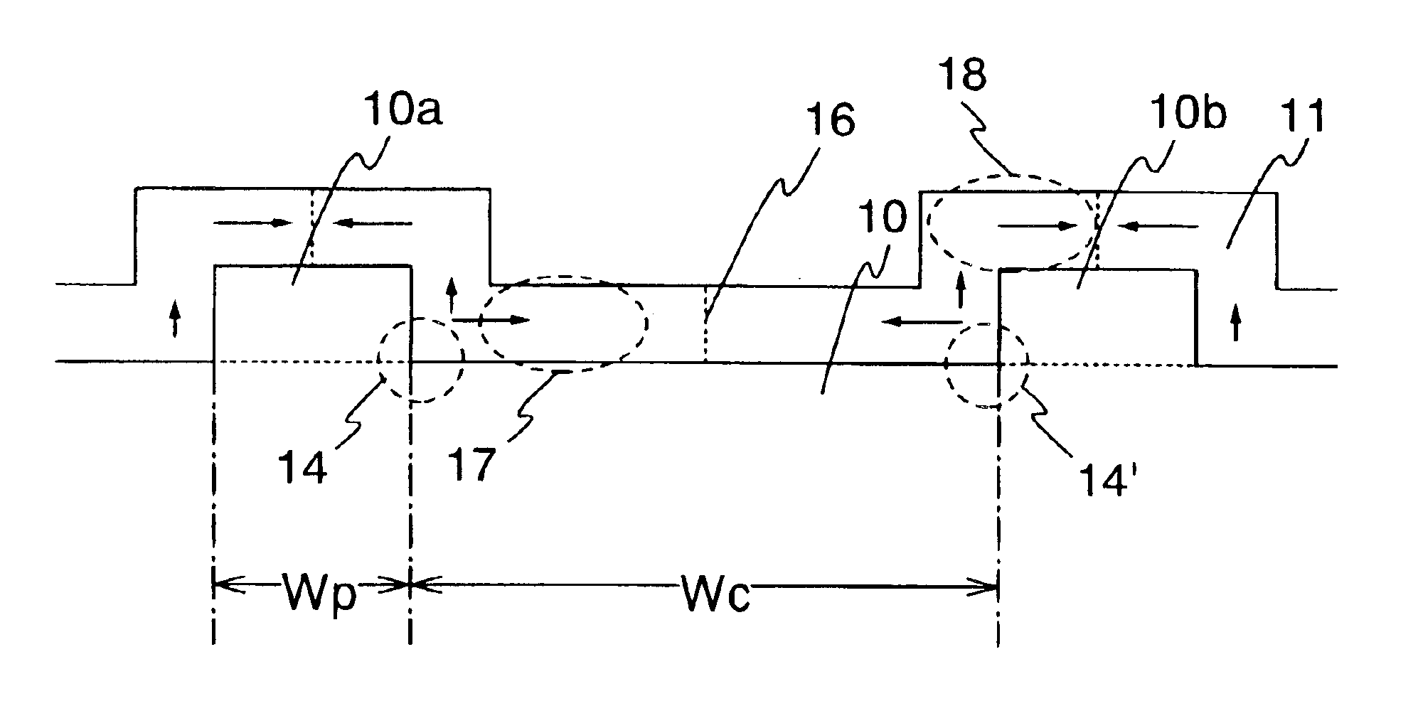
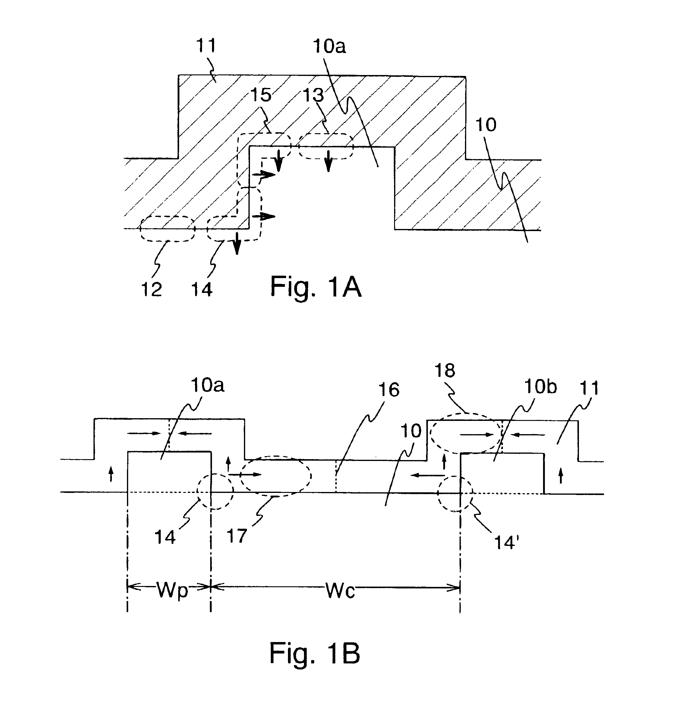
This embodiment explains how to form an insulating film having depression / projection.
At first, a first insulating film 251 is formed on a substrate 250, as shown in FIG. 8A. Although the first insulating film 251 uses siliconoxidenitride in this embodiment, this is not limited to, i.e. an insulating film having a great etching selective ratio to a second insulating film is satisfactory. In this embodiment, the first insulating film 251 was formed to a thickness of 50-200 nm using SiH4 and N2O by a CVD apparatus. Note that the first insulating film may be of a single layer or a layered structure having a plurality of insulating films.
Then, a second insulating film 252 is formed in contact with the first insulating film 251, as shown in FIG. 8B. The second insulating film 252 requires a film thickness to a degree that, when a depression-projection is formed thereon by patterning in a subsequent process, the depression-projection appears on a surface of a semiconductor film to be sub...
embodiment 2
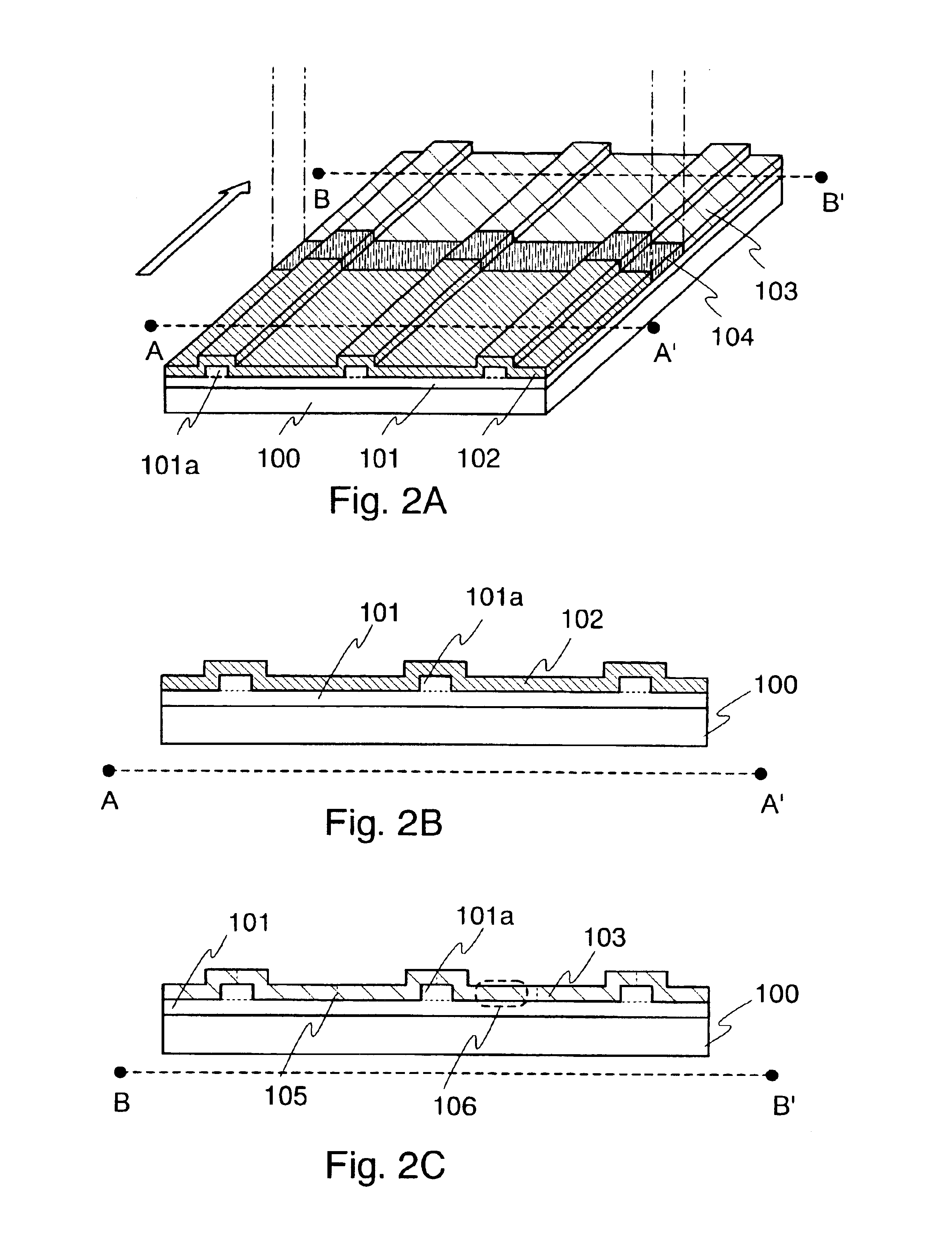
This embodiment explains an example that a semiconductor film formed on an insulating film in a stripe form is crystallized by laser light irradiation and thereafter mutually isolated islands are formed on a surface parallel with an projection-formed substrate to fabricate TFT using the islands.
FIG. 10A shows a TFT structure of this embodiment. In FIG. 10A, an insulating film 152 having striped projection parts 151 is formed on a substrate 150. A plurality of islands 153 are formed, isolated from one another, on the top surfaces of the projection parts 151. An gate insulating film 154 is formed in a manner contacting with the islands 153. Incidentally, although the gate insulating film 154 in FIG. 10A is formed exposing the regions, to be made into impurity regions, of the island, it may be formed covering the entire island 154.
A plurality of gate electrodes 155 is formed on the gate insulating film 154 in a manner superposed over a plurality of islands 153. The plurality of gate el...
embodiment 3
This embodiment explains variations of insulating film forms.
FIG. 11A shows an embodiment on an insulating film form of the invention. In FIG. 11A, an insulating film 171 is formed on a substrate 170 wherein the insulating film 171 has a plurality of projection parts 172. The projection part 172 is rectangular in form as viewed from the above. All the projection parts have respective rectangular longer or shorter sides in a direction parallel with a scanning direction of laser light shown by the arrow.
The projection parts 172 are not necessarily identical to one another in the width in laser-light scanning direction and the width perpendicular to the scanning direction. A form of an insulating film is desirably designed to meet a desired island form.
It is not necessary that projection parts of the insulating film using the present invention being completely striped. It is need only a portion of the insulating film is striped or rectangular. FIG. 11B shows an embodiment on an insulat...
PUM
Property
Measurement
Unit
Concentration
aaaaa
aaaaa
Abstract
A semiconductor device production system using a lasercrystallization method is provided which can avoid forming grain boundaries in a channel formation region of a TFT, thereby preventing grain boundaries from lowering the mobility of the TFT greatly, from lowering ON current, and from increasing OFF current. Rectangular or stripe pattern depression and projection portions are formed on an insulating film. A semiconductor film is formed on the insulating film. The semiconductor film is irradiated with continuous wavelaser light by running the laser light along the stripe pattern depression and projection portions of the insulating film or along the major or minor axis direction of the rectangle. Although continuous wavelaser light is most preferred among laser light, it is also possible to use pulse oscillation laser light in irradiating the semiconductor film.
Description
BACKGROUND OF THE INVENTION1. Field of the InventionThe present invention relates to a semiconductor device constructed by a semiconductor film that has a crystal structure, and more specifically, to a semiconductor device using a thin film transistor whose active layer is formed of a crystalline semiconductor film obtained through crystal growth on an insulating surface. The present invention also relates to a semiconductor device product ionsystem using laser light.2. Description of the Related ArtIn recent years, techniques for forming TFTs on a substrate have made great advancements and applications of TFTs to active matrix type semiconductor display devices are being developed. In particular, TFTs formed of polycrystalline semiconductor films (hereinafter referred to as polysilicon TFT) have higher field effect mobility (also referred to as mobility) than conventional TFTs that use amorphous semiconductor films, and accordingly can operate at high speed. Therefore pixels can b...
Claims
Application Information
Patent Timeline
Application Date:The date an application was filed.
Publication Date:The date a patent or application was officially published.
First Publication Date:The earliest publication date of a patent with the same application number.
Issue Date:Publication date of the patent grant document.
PCT Entry Date:The Entry date of PCT National Phase.
Estimated Expiry Date:The statutory expiry date of a patent right according to the Patent Law, and it is the longest term of protection that the patent right can achieve without the termination of the patent right due to other reasons(Term extension factor has been taken into account ).
Invalid Date:Actual expiry date is based on effective date or publication date of legal transaction data of invalid patent.

