Process for low-temperature metal-organic chemical vapor deposition of tungsten nitride and tungsten nitride films

a technology of metal-organic chemical vapor deposition and tungsten nitride, which is applied in the direction of coatings, chemistry apparatus and processes, layered products, etc., can solve the problems of limited application of sputtering techniques, further complicated needs, and inability to achieve high conformality with low impurities

Inactive Publication Date: 2005-04-26
GELEST +1
View PDF53 Cites 96 Cited by
  • Summary
  • Abstract
  • Description
  • Claims
  • Application Information

AI Technical Summary

Benefits of technology

[0024]The foregoing summary, as well as the following detailed description of preferred embodiments of the invention, will be better understood when read in conjunction with the appended drawings. For the purpose of illustrating the invention, there is shown in the drawings embodiments which are presently preferred. It should be understood, however, that the invention is not limited to the precise arrangements and instrumentalities shown. In the drawings:
[0025]FIG. 1 is a representation of high resolution x-ray photoelectron spectroscopy (XPS) spectra of the W4f7 / 2 elemental core peaks for (a) metal-organic chemical vapor deposition (MOCVD) W2N films formed in accordance with an embodiment of the process of the invention in Example 1 and (b) a sputtered pure W standard;

Problems solved by technology

These needs are further complicated by the on-going transition from aluminum-based to copper-based metallization schemes, and requires exploring new candidate liner materials that are chemically and thermodynamically more stable towards copper diffusion and migration than the presently used titanium / titanium nitride materials.
While WNx presents a potentially viable solution given its attractive properties as highly refractory material with excellent mechanical and chemical properties, there remains problems with achieving high conformality with low impurities.
Unfortunately, the application of sputtering techniques is limited by concerns over the ability to provide good conformality in sub-100 nm device structures.
While such CVD-based methods could provide viable step coverage in such aggressive topographies, thereby allowing the potential use of the same CVD liner technology in multiple generations of sub-100 nm microprocessor and memory products, inorganic CVD from WF6 and NH3 poses challenges.
The difficulties include: (a) transport and handling concerns attributed to the high reactivity of the fluorinated WF6 source, (b) process concerns caused by potential gas phase particle generation in the reaction of WF6 and NH3 and (c) reliability issues pertaining to the possible inclusion of fluorine in the resulting WNx liner which is a fast diffuser in metals such as copper.
At temperatures of about 450° C. and higher, the hydrocarbon-based ligands in such sources tend to decompose readily, leading to film contamination with carbon and, as a result, higher resistivity.
Dimethylamido-substituted tungsten compounds have been shown in model studies not to be stable enough to volatilize or undergo transport without vapor phase particle formation, which is inconsistent with the formation of uniform coatings.
Unfortunately, the ALCVD approaches described in the prior art have not successfully reported the growth of WNx films with electronic grade quality for microelectronics applications, in part due to the lack of an appropriate metal-organic source chemistry which is amenable to the self-limiting adsorption in monolayer form on the substrate surface.
In addition, the high chemical and thermal instability of many of the metal-organic tungsten source precursors used in the prior art can cause premature decomposition of the source chemistry upon contact with the substrate surface.
Even in the case of the inorganic tungsten hexafluoride source chemistry, there has not been a successful identification of an appropriate process window and / or intermediate precursor species that can successfully and reliably allow adsorption and decomposition in a layer-by-layer ALD mode.

Method used


Image

  • Process for low-temperature metal-organic chemical vapor deposition of tungsten nitride and tungsten nitride films
  • Process for low-temperature metal-organic chemical vapor deposition of tungsten nitride and tungsten nitride films
  • Process for low-temperature metal-organic chemical vapor deposition of tungsten nitride and tungsten nitride films

Examples


example 1

[0102]An alpha-type, 200 mm-wafer, cold-wall, plasma-capable CVD reactor, equipped with a high vacuum loadlock for wafer transport and handling was used in this Example. The use of the loadlock system allowed for tight control over the cleanliness of the CVD chamber, and prevented undesirable contamination from exposure to ambient conditions during sample loading and unloading. In addition, a cryogenic pump was used to routinely achieve a chamber base pressure at about 10−6 torr, while a roots blower pumping stack was used during actual growth runs. The precursor was placed in a reservoir heated to temperatures ranging from 85 to 100° C., depending on the processing conditions, and the precursor flow rate into the reactor was regulated by an MKS 1153 solid source delivery system (SSDS). The SSDS and all delivery lines were heated to 120° C. to prevent precursor recondensation.

[0103]Parallel plate, radio-frequency plasma (13.56 MHz) capability was used for in situ, pre-deposition, wa...

example 2

[0113]In this Example, the same procedures were used as described above in Example 1 in detail with the exception that in this Example, thermal deposition of a number of tungsten nitride films was carried out using a stand-alone single module deposition chamber and reacting tungsten hexacarbonyl with ammonia in the presence of hydrogen gas. The reaction parameters are shown below in Table 2.

[0114]

TABLE 2Parameter NameParameter in Example 2Substrate Temperature220° C.Ammonia Flow Rate 100 standard cm3 / minHydrogen Flow Rate  50 standard cm3 / minProcess Pressure0.5 torrPrecursor Flow Rate18.7 standard cm3 / minDeposition Rate2 nm / min

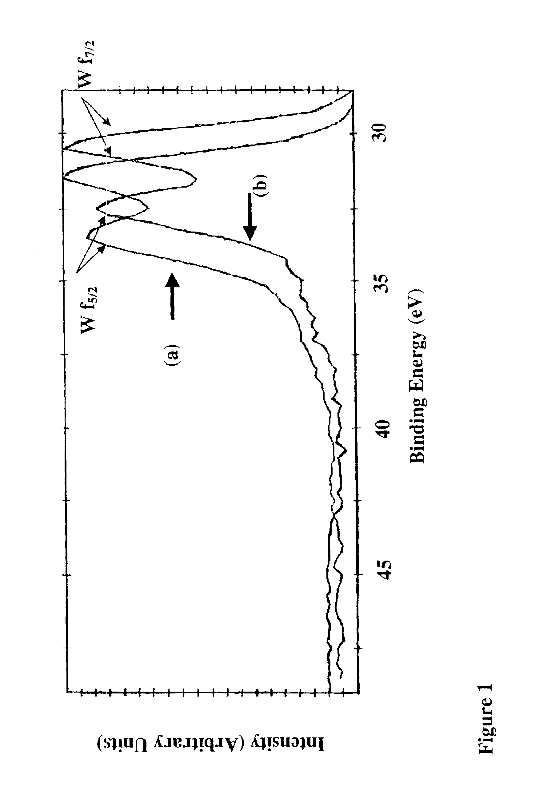
[0115]Using the above parameters, the following tests as set forth in Table 3 below, which are described in further detail in Example 1 were carried out and demonstrate that amorphous W2N films were formed with less than about 5 at % hydrogen, about 5-8 at % oxygen, and about 4-6 at % carbon. The relevant representative spectra for this Example are shown in FI...

example 3

[0117]In this Example, the procedure of Example 1 was followed with the exception that thermal CVD of tungsten nitride films was undertaken using a cluster tool platform. The reactants were tungsten hexacarbonyl and ammonia. The reaction conditions are shown below in Table 4.

[0118]

TABLE 4Parameter NameParameter in Example 3Substrate Temperature225° C.Ammonia Flow Rate150 standard cm3 / minHydrogen Flow Rate—Process Pressure0.5 torrPrecursor Flow Rate 20 standard cm3 / minDeposition Rate4 nm / min

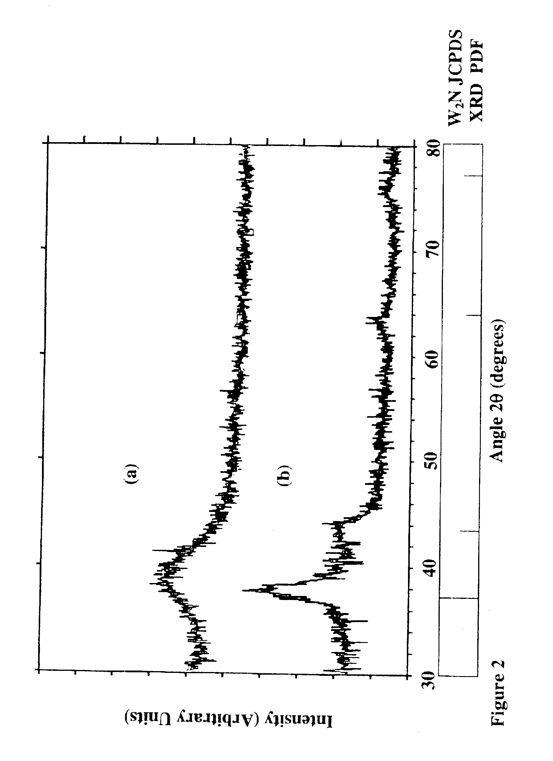
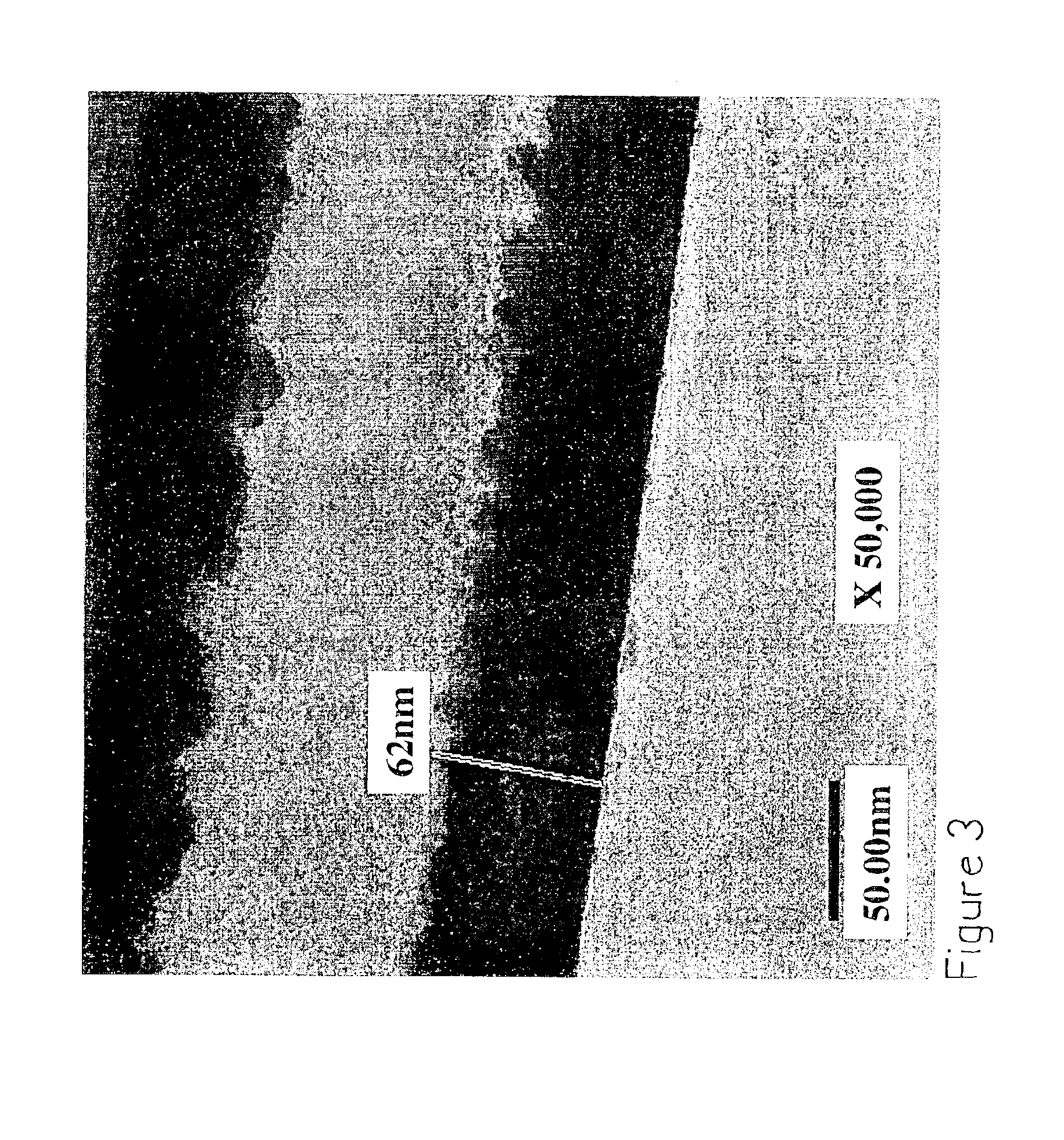
[0119]The resulting films and coated substrates formed using the above parameters were tungsten nitride films of varied compositions within the formula WNx where 0.1≦x≦2.0. The oxygen and carbon impurities were less than about 1-3 at % O and less than about 1-2 at % carbon with no hydrogen. The resulting phases of the different films varied from amorphous to amorphous with partial polycrystallinity in a β-phase. FIGS. 11-14 show the characteristics of the films. The resisitivities were measured to...


PUM

PropertyMeasurementUnit
temperatureaaaaaaaaaa

Abstract

Processes for producing tungsten nitride and tungsten nitride films are provided in which a tungsten carbonyl compound and a nitrogen-containing reactant gas are reacted at a temperature below about 600° C. Tungsten nitride precursors are also included which comprise a tungsten carbonyl compound capable of forming a tungsten nitride film in the presence of a nitrogen-containing reactant gas at a temperature of less than about 600° C. A process for forming a film by atomic layer deposition is also provided which includes introducing a substrate having a surface into a deposition chamber and heating the substrate to a temperature sufficient to allow adsorption of a tungsten source precursor or an intermediate thereof, and thereafter sequentially introducing by pulsing: a tungsten source precursor which is absorbed as a monolayer, a purging inert gas, a nitrogen-containing gas for reacting with the monolayer to form a first tungsten nitride layer on the substrate surface, and an inert purging gas, and repeating the sequence to form a film of desired thickness.

Description

CROSS-REFERENCE TO RELATED APPLICATIONS[0001]This application is a continuation of U.S. patent application Ser. No. 09 / 502,260, filed Feb. 11, 2000 now abandoned, further claims the benefit of U.S. Provisional Application No. 60 / 119,957, filed Feb. 12, 1999, the entire disclosures of these applications are hereby incorporated by reference.BACKGROUND OF THE INVENTION[0002]As computer chip device dimensions continue their evolution towards feature sizes below 100 nm, new liner materials and associated process technologies are needed to ensure viable diffusion barrier and adhesion promoter performance between the conductor and the surrounding regions of silicon-based and dielectric-based materials. These liners must possess mechanical and structural integrity, good conformality within aggressive device features, high conductivity to minimize plug overall effective resistance, and thermal, mechanical, and electrical compatibility with neighboring conductor and dielectric material system...

Claims


Application Information

Patent Timeline
Patent Type & Authority Patents(United States)
IPC IPC(8): C01B21/00C01B21/06C23C16/34B32B9/00
CPCC01B21/062C23C16/34C01P2002/72C01P2002/77C01P2004/04C01P2006/10C01P2006/40C01P2004/03B32B9/00
Inventor KALOYEROS, ALAIN E.ARKLES, BARRY C.
Owner GELEST
Why Eureka
Try Eureka