Copper nanocrystals and methods of producing same

a technology of copper nanocrystals and nanocrystals, which is applied in the field of copper nanocrystals and methods of producing same, can solve the problems of degrading the fine architecture structure of the substrate, increasing the difficulty of designing and fabricating and increasing the difficulty of manufacturing ultralarge scale integrated circuit chips. achieve the effect of reducing copper

Inactive Publication Date: 2005-05-03
WAYNE STATE UNIV
View PDF19 Cites 83 Cited by
  • Summary
  • Abstract
  • Description
  • Claims
  • Application Information

AI Technical Summary

Problems solved by technology

It is becoming increasingly difficult to design and fabricate ultralarge scale integrated circuits (ULSI) chips with the desired high packing density and high-speed operation.
This is not due to the difficulty of transistor scaling but to the interconnect delay in distributing high frequency signals across the ULSI chip.
The process is cumbersome in terms of time, money and energy.
Additionally, heating of the IC substrate during CVD to assure crystalline growth degrades fine architecture structures on the substrate.
In addition to the high purchase cost of a separate chamber to perform each of these additional steps, each step adds about $1 per metallization layer in consumable materials cost.
Mesoscopic systems exhibit collective atomic behavior, but not to a sufficient extent so as to preclude quantized effects.
The reduction in melting temperature as a function of nanocrystal size can be enormous.
Silver nanoparticle syntheses are only to a very limited extent adapable to making Cu nanocrystals.
Inherent inadequacies in conventional nanoparticle synthesis technology with respect to polydispersity and solubility, preclude the formation of high conductivity interconnects necessary for internal communication within an IC.
For example, the polydispersity of Cu nanocrystals made by conventional methodology, results in a broad range of melting temperatures and leads to comparatively high resitivity in interfacial regions between particles melting at variable temperatures.
Unsuccessful attempts have been made to obtain Cu nanocrystals involving a number of methodologies.
Additionally, hydrazine carboxylate and complexes thereof are potentially explosive making them diffuclt to work with.
As such, this method is not capable of forming suitable nanocrystal colloids.
However, the sulfur-containing set of passivating agents / ligands was ultimately abandoned when it became apparent that nanocrystals passivated by such ligands led to Cu2S or Cu2S / Cu mixtures under thermolysis conditions.
The amount of soluble material present was certainly so miniscule (probably microgram scale) that any application of such nanocrystals would be impossible.

Method used


Image

  • Copper nanocrystals and methods of producing same
  • Copper nanocrystals and methods of producing same
  • Copper nanocrystals and methods of producing same

Examples


example 1

[0065]Synthesis and Characterization of Copper Nanocrystals Procedure 1A using 1-decyl-2-methylimidazole as passivating Agent: Under argon and at room temperature 20 mL of pyridine was added to a vigorously stirred 0.25 M pale blue solution of copper nitrate (25 mL, 6.25 mmol) and the color immediately became deep blue. Hexanes (50 mL) was then added. To the mixture a freshly prepared solution of NaBH4 (0.60 g) in water (40 mL) was added dropwise in a period of 15 minutes and further stirring was continued for another 15 minutes to afford a (red) brown mixture. If stirring was stopped a brown aqueous phase and a colorless hexanes phase could be observed. To the stirred red-brown mixture 1-heptyl-4-(4pyridyl)pyridium bromide (0.697 g, 2.08 mmol, from Aldrich) was added and stirred for 30 minutes followed by addition of 1-decyl-2-methylimidazole (0.700 g, 3.125 mmol, from Aldrich) and stirring for half an hour. Black insoluble material was formed in the aqueous phase and partially pre...

example 2

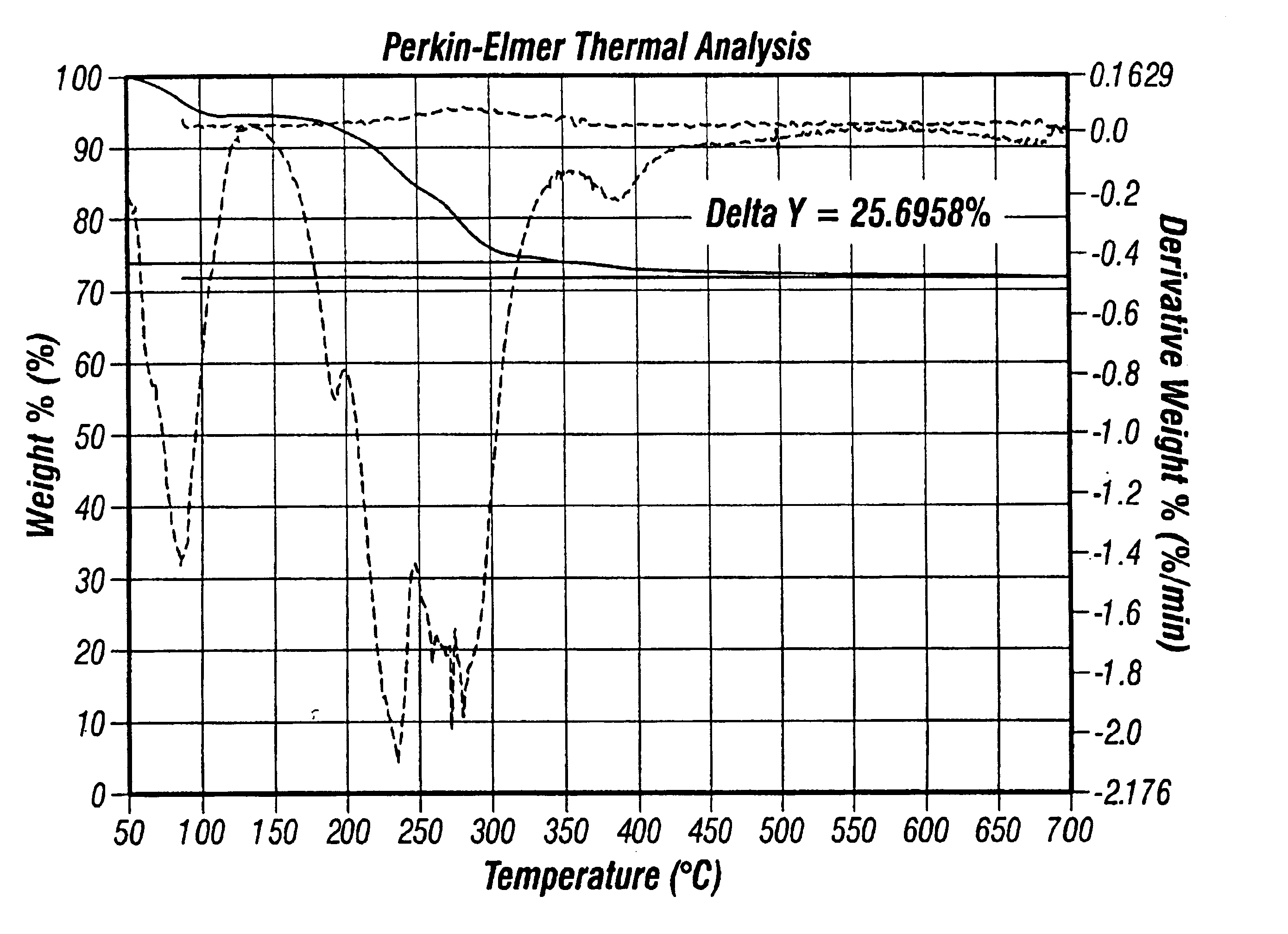
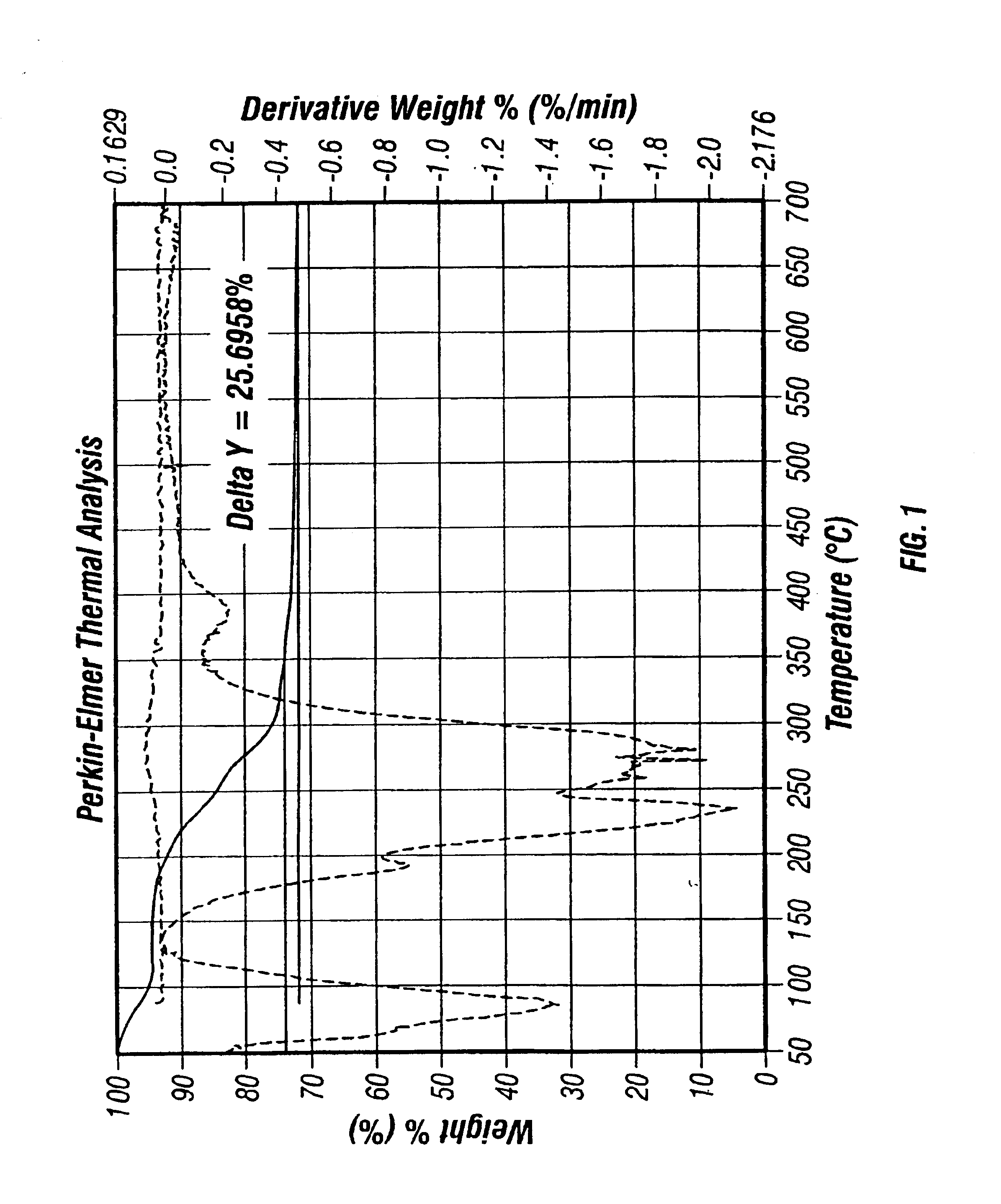
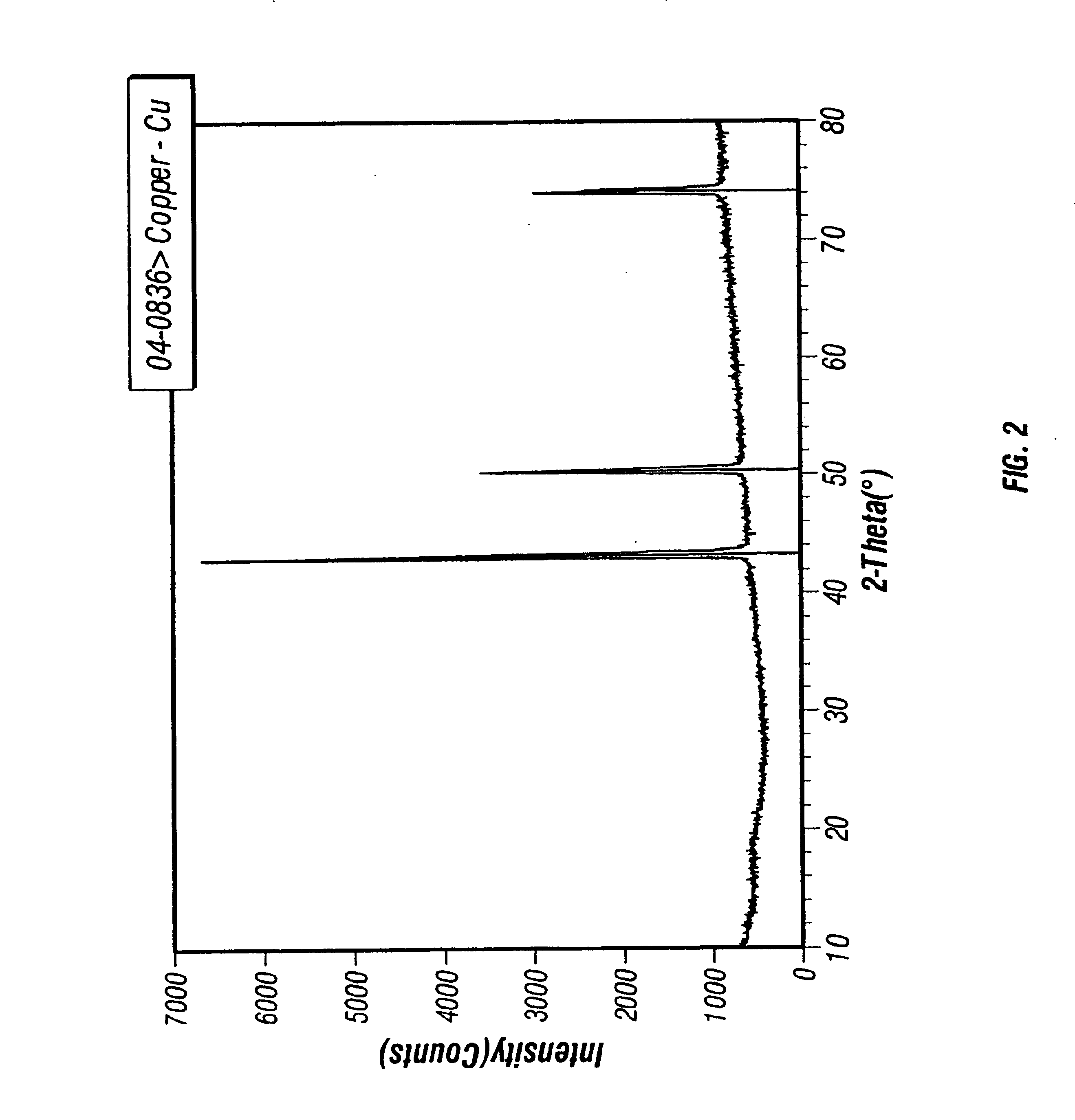
[0073]Copper Films from the Passivated Nanocrystals. Synthesis of 5.5±1.0 nm copper nanocrystals are passivated with either tetra-n-octylammonium decanoate or 1-decyl-2-methylimidazole. These copper nanocrystals melt at about 350° C., exhibit X-ray diffraction spectra consistent with copper metal, and are highly soluble (up to 10 wt. %) in organic solvents ranging from n-alkanes to ethyl lactate. Thermolysis of the nanocrystals at 350° C. under a nitrogen / hydrogen atmosphere afforded pure copper metal, with complete evaporation of the passivating agents. Weight loss upon heating, as measured by thermogravimetric analysis, was 27-32%. Thermogravimetric analysis also indicated that evaporation of the passivating agents occurs between 150-250° C. A 6 wt. % dodecane solution of 5.5±1.0 nm tetra-n-octylammonium decanoate-passivated copper nanocrystals was spin coated onto a TaN-coated (1000 Å by PVD) flat silicon wafer. Spin coating of nanocrystal solutions onto a TaN-coated silicon wafe...

example 3

[0074]Spin Coating and Heating of the Passivated Nanocrystals. A dilute (<1 wt. %) pyridine solution of copper nanocrystals is spin coated onto a silicon wafer containing an array of 0.1×1.0 μm blind vias. Notably, substrates that are heated to about 300° C. do not have a continuous copper film on the substrate plateau. The substrate following nanocrystal deposition prior to heating shows completely conformal coverage of the vias and plateau region. Upon heating to 150° C., wicking of nanoparticles from the plateau region to the via is observed. At about 300° C., a perfectly conformal copper film has been obtained in the via.


PUM

PropertyMeasurementUnit
sizeaaaaaaaaaa
diameteraaaaaaaaaa
sizeaaaaaaaaaa

Abstract

The invention relates to methods of making monodisperse nanocrystals comprising the steps of reducing a copper salt with a reducing agent, providing a passivating agent comprising a nitrogen and / or an oxygen donating moitey and isolating the copper nanocrystals. Moreover, the invention relates to methods for making a copper film comprising the steps of applying a solvent comprising copper nanocrystals onto a substrate and heating the substrate to form a film of continuous bulk copper from said nanocrystals. Finally, the invention also relates to methods for filling a feature on a substrate with copper comprising the steps of applying a solvent comprising copper nanocrystals onto the featured substrate and heating the substrate to fill the feature by forming continuous bulk copper in the feature.

Description

FIELD OF THE INVENTION[0001]The invention relates to methods of making macroscopic quantities of monodisperse, soluble copper nanocrystals. The present invention also relates to microelectronic trenched feature formation and more particularly to the formation of an interconnect from a copper nanocrystal solution.BACKGROUND OF THE INVENTION[0002]An integrated circuit requires conductive interconnects between semiconducting domains in order to communicate signals therebetween. In order to create ever faster microprocessors, smaller dimension interconnects of higher conductivity materials is an ongoing goal.[0003]As microelectronic efficiencies have increased, interconnects have decreased in dimensional size and efforts have been made to increase the electrical conductivity of interconnect features. It is becoming increasingly difficult to design and fabricate ultralarge scale integrated circuits (ULSI) chips with the desired high packing density and high-speed operation. This is not d...

Claims


Application Information

Patent Timeline
Patent Type & Authority Patents(United States)
IPC IPC(8): B22F9/24B22F1/00B22F9/16B22F1/054B22F1/10B22F1/102B22F1/145
CPCB22F1/0018B22F1/0059B22F1/0062B22F1/0088B22F9/24B82Y30/00B22F2998/00B22F2999/00B22F1/102B22F1/054B22F1/10B22F1/145
Inventor WINTER, CHARLES H.YU, ZHENGKUNDEZELAH, IV, CHARLES L.
Owner WAYNE STATE UNIV
Why Eureka
Try Eureka