

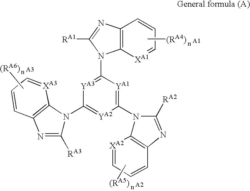
Light emitting element and azole compound
a technology of light-emitting elements and compound compounds, which is applied in the direction of discharge tube luminescnet screens, natural mineral layered products, transportation and packaging, etc., can solve the problems of inferior emission illuminance and luminance efficiency of elements produced by a conventional coating method to elements produced by a deposition system, and achieve high luminance efficiency, high color purity, and high luminance efficiency.
- Summary
- Abstract
- Description
- Claims
- Application Information
AI Technical Summary
Benefits of technology
Problems solved by technology
Method used
Image

Examples
synthesis example 1
Synthesis of Exemplified Compound A-7
[0113]3.17 g (8.0 mmol) of 1,3,5-tris(2-aminophenylamino)benzene was dissolved in 50 ml of dimethylacetoamide, and 5 ml (36 mmol) of triethylamine was added thereto under an atmosphere of nitrogen. After cooling to the temperature of 0° C. or lower, 2.0 ml (26.4 mmol) of acetylchloride was gently dropped into the mixture so as to maintain the temperature of 0° C. or lower. About one hour after the dropping was completed, the temperature was maintained at 0° C. or lower, and the temperature was gradually raised and the resulting product was stirred for 5 hours. A reaction solution was poured into 300 ml of water and a solid matter thus deposited was filtered out and washed with water. The obtained solid matter, 1 g of p-toluene sulfonic acid monohydrate, and 100 ml of xylene were heat-refluxed for about 10 hours. The solvent was removed under a reduced pressure, and thereafter, a condensate thus obtained was purified with silica gel column chromat...
synthesis example 2
Synthesis of Exemplified Compound A-19
[0114]3.69 g (20 mmol) of cyanuric chloride, 8.72 g (66 mmol) of 2-methylbenzimidazole, 41.6 g (180 mmol) of rubidium carbonate, 0.135 g (0.6 mmol) of palladium acetate, 0.44 ml (1.8 mmol) of tri-tert-butylphosphine, and 70 ml of o-xylene were mixed and heated under an atmosphere of nitrogen at 120° C. for 6 hours. After cooling to room temperature, a solid matter was filtered out, and washed with chloroform. An organic layer thus formed was washed with water, and thereafter, dried with magnesium sulfuric anhydride, and the solvent was removed under a reduced pressure. The condensate was purified with silica gel column chromatography (eluent: chloroform / methanol=100 / 1 (vol / vol)), and thereafter, recrystallized with ethyl acetate to obtain 2.5 g (5.32 mmol) of the exemplified compound A-19 (yield: 27%).
[0115]The aforementioned luminescent material contains at least one compound having a light emission maximum wavelength from an exciton in the blu...
example 1
[0148]An ITO substrate which was washed was placed in an evaporating apparatus and α-NPD(N,N′-diphenyl-N,N′-di(α-naphthyl)-benzidine) was deposited on the substrate in a thickness of 50 nm. CBP (biscarbazolylbenzidine) and the exemplified compound K-1 were co-deposited thereon in a ratio of 17:1 in a thickness of 36 nm. The exemplified compound B-40 was further deposited thereon in a thickness of 24 nm. A patterned mask (the emission area was designed to be 4 mm×5 mm) was placed on the organic thin film to co-deposit magnesium / silver (10:1) in a thickness of 250 nm. Thereafter, silver was deposited in a thickness of 300 nm to produce a light emitting element.
PUM
| Property | Measurement | Unit |
|---|---|---|
| Fraction | aaaaa | aaaaa |
| Fraction | aaaaa | aaaaa |
| Fraction | aaaaa | aaaaa |
Abstract
Description
Claims
Application Information