
Method for manufacturing a ruthenium film for a semiconductor device

Inactive Publication Date: 2006-01-24
RENESAS ELECTRONICS CORP
View PDF23 Cites 3 Cited by
  • Summary
  • Abstract
  • Description
  • Claims
  • Application Information

AI Technical Summary

Benefits of technology

[0015]As has been described above, no ruthenium film is deposited on the side wall of a deep hole by the existent sputtering method. However, it has been found that the ruthenium film can be deposited also on the side wall of the deep hole by using low-pressure and long-throw sputtering. This is a method of taking a long distance between a target and a substrate and lowering the pressure of a sputtering atmosphere thereby enhancing the straight forwarding property of sputtering particles. By the method, the sputtered particles can reach the inside of the deep hole.
[0016]Further, as the method of enhancing the straight forwarding property of the sputtering particles, similar effect can be obtained, not restricted to the low-pressure and long-throw sputtering, also by collimated sputtering of locating a collimator between a target and a substrate or an ionized sputtering of ionizing sputtering particles and unifying the forwarding direction by an electric field.
[0018]On the other hand, in a case of the low-pressure and long-throw sputtering, since sputtering particles have high kinetic energy, adhesion between the lower ruthenium electrode and SiO2 can be increased due to collision against the underlying layer.
[0028]After fabricating an interlayer insulating film such that an opening has a circular cylindrical, elliptic cylindrical or square cylindrical shape, a lower ruthenium electrode is deposited by low-pressure and long-throw sputtering over the entire surface such that the film thickness on the side wall of the deep hole is about 20 nm. Since the lower electrode formed by sputtering has high adhesion with the underlying portion, peeling can be suppressed.
[0034]After fabricating an interlayer insulating film such that an opening forms a circular cylindrical shape, elliptic cylindrical or square cylindrical, a lower ruthenium electrode is deposited by low-pressure and long-throw sputtering over the entire surface such that the film thickness on the side wall of the deep hole is about 20 nm. Since the lower electrode formed by sputtering has high adhesion with the underlying portion, peeling can be suppressed.
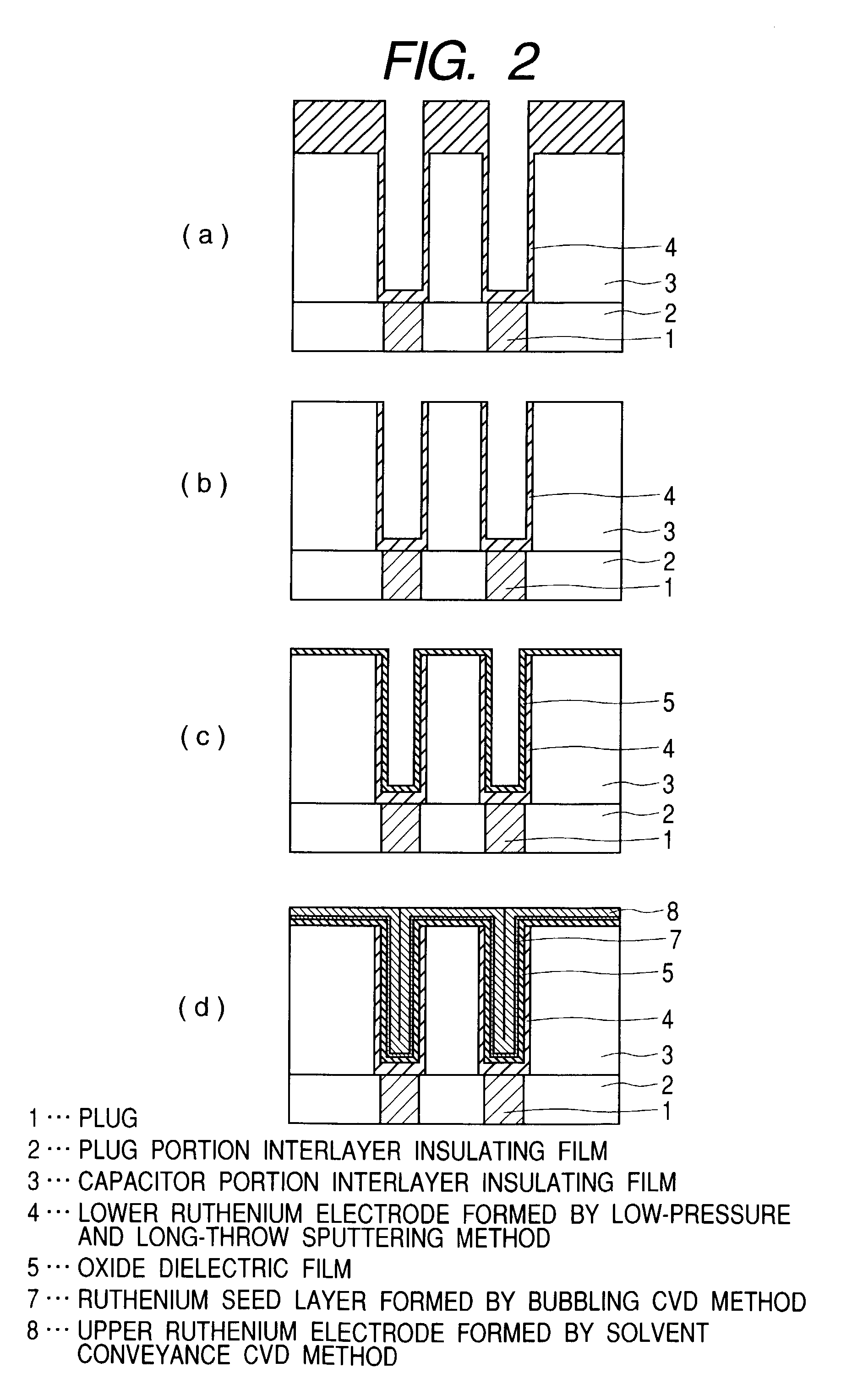
[0037]Then, a step of depositing an upper ruthenium electrode is necessary. The step of using, for example, Ru(EtCp)2 as the starting material and depositing the upper ruthenium electrode by chemical vapor deposition using the bubbling or liquid conveyance method has been described previously. However, the method described above, since the methods described above convey the starting material directly, they involve a problem that the thickness of the ruthenium film tends to fluctuates depending on the temperature of the starting material container or pipelines. Further, when the viscosity of the starting material is high, the starting material may possibly cause clogging to valves or pipeline portions. Accordingly, as a method capable of stably supplying the starting material, the solvent conveyance method is used preferably. The solvent conveying method also has a merit capable of using a solid organic compound starting material. However, a ruthenium seed layer is necessary for obtaining good coverage as described above. Then, after the deposition of the dielectric material, a ultra-thin ruthenium film is deposited over the entire surface by chemical vapor deposition of conveying the starting material (bubbling or liquid conveyance method). This is referred to as a seed layer. The seed layer functions well even when it is a discontinuous film of about 1 nm thickness. When the thickness of the seed layer fluctuates, the function does not change. Further, since the film thickness is thin, the amount of the starting material to be used can be reduced. Accordingly, the problem that the film thickness tends to fluctuate and the starting material may possibly cause clogging in the valve or the like in the bubbling or liquid conveyance method is negligible. An upper ruthenium electrode of a desired film thickness is deposited on the seed layer by chemical vapor deposition of using the solvent conveyance method. So long as it is on the seed layer, an upper ruthenium of high coverage can be formed also by the solvent conveyance method.

Problems solved by technology

The ruthenium film can be deposited with good coverage also by using chemical vapor deposition to be described later but, since the ruthenium formed by the chemical vapor deposition has poor adhesion with the underlying SiO2, peeling occurs when it is used as a lower electrode of a capacitor.

Method used


Image

  • Method for manufacturing a ruthenium film for a semiconductor device
  • Method for manufacturing a ruthenium film for a semiconductor device
  • Method for manufacturing a ruthenium film for a semiconductor device

Examples


embodiment 1

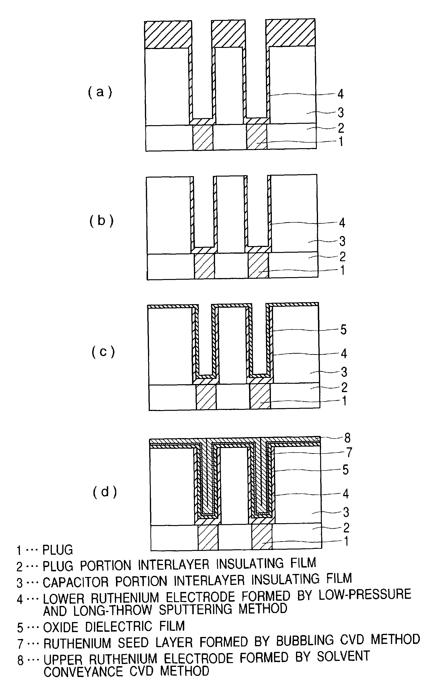
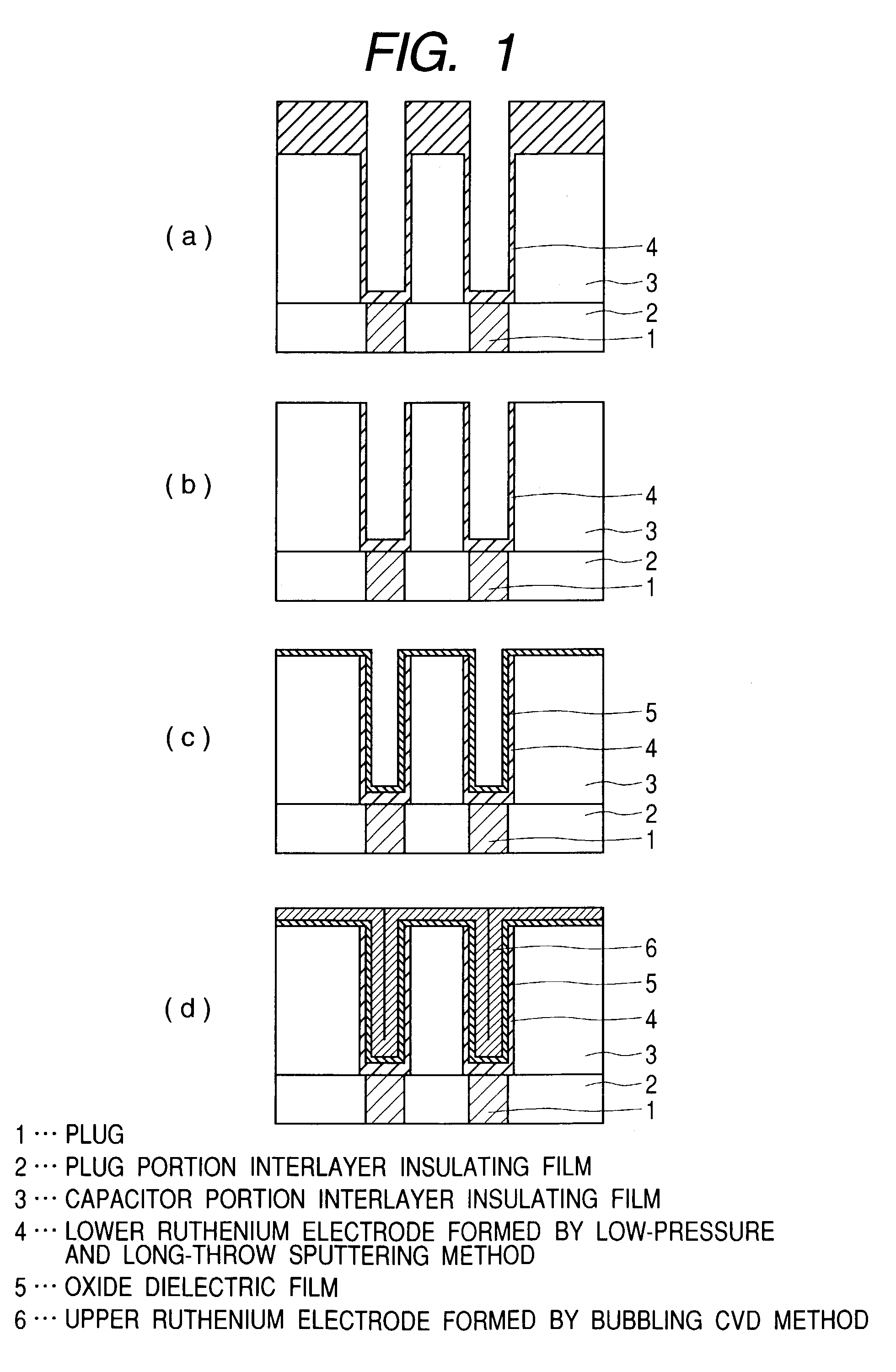
[0059]Embodiment 1 according to this invention is to be described with reference to FIG. 1. In this embodiment, a lower ruthenium electrode is formed by low-pressure and long-throw sputtering and an upper ruthenium electrode is formed by chemical vapor deposition of conveying a starting material.

[0060]At first, on plugs 1 comprising titanium nitride and a plug portion interlayer insulating film 2 comprising SiO2, a capacitor portion interlayer insulating film 3 of 700 nm thickness comprising SiO2 was deposited by plasma CVD using a mono-silane gas as a starting material.

[0061]Then, resist was coated and developed by well-known photolithography and the capacitor portion interlayer insulating film 3 was fabricated by dry etching as far as the surface of the plug 1 using the resist as a mask. The fabrication was applied such that the opening had an elliptic cylindrical shape, and the opening is utilized as a lower electrode.

[0062]After removing the resist, a lower ruthenium electrode 4...

embodiment 2

[0073]Embodiment 2 according to this invention is to be described with reference to FIG. 2. In this embodiment, a lower ruthenium electrode is formed by low-pressure and long-throw sputtering, forming a ruthenium seed layer by chemical vapor deposition of conveying the starting material and then an upper ruthenium electrode is formed by chemical vapor deposition of conveying a starting material dissolved in a solvent.

[0074]At first, a capacitor portion interlayer insulating film 3 of 700 nm thickness comprising SiO2 was deposited on plugs 1 comprising titanium nitride and a plug portion interlayer insulating film 2 comprising SiO2 by plasma CVD using a mono-silane gas as the starting material.

[0075]Then, a resist was coated and developed by well-known photolithography, and a capacitor portion interlayer insulating film 3 was fabricated as far as the surface of the plugs 1 by dry etching using the resist as a mask. The fabrication was made such that the opening has an elliptic cylind...

embodiment 3

[0089]Embodiment 3 of this invention is to be described with reference to FIG. 3. This embodiment is adapted for forming a ruthenium seed layer by low-pressure and long-throw sputtering, and then forming a lower ruthenium electrode by chemical vapor deposition of conveying the starting material dissolved in a solvent, forming an upper ruthenium electrode by chemical vapor deposition of conveying the starting material.

[0090]At first, on plugs 1 comprising titanium nitride and a plug portion interlayer insulating film 2 comprising SiO2, a capacitor portion interlayer insulating film 3 of 700 nm thickness comprising SiO2 was deposited by a plasma CVD method using a mono-silane gas as a starting material.

[0091]Subsequently, resist was coated and developed by well-known photolithography and the capacitor portion interlayer insulating film 3 was fabricated as far as the surf ace of the plugs 1 by dry etching using the resist as a mask. Fabrication was conducted such that the opening had a...


PUM

PropertyMeasurementUnit
Temperatureaaaaaaaaaa

Abstract

In the method of manufacturing a semiconductor device according to this invention, when an interlayer insulating film is fabricated such that an opening is cylindrical and low-pressure and long-throw sputtering is used for forming a lower ruthenium electrode, a ruthenium film can be deposited on the side wall of a deep hole. Further, after removing the ruthenium film deposited on the upper surface of the interlayer insulating film, a dielectric material comprising, for example, a tantalum pentoxide film is deposited. Successively, an upper ruthenium electrode is deposited using, for example, Ru(EtCp)2 as a starting material and by chemical vapor deposition of conveying the starting material by bubbling. The upper ruthenium electrode can be formed with good coverage by using conditions that the deposition rate of the ruthenium film depends on the formation temperature (reaction controlling condition). This invention can provide a fine concave type capacitor having a ruthenium electrode.

Description

TECHNICAL FIELD[0001]The present invention concerns a semiconductor device using ruthenium as an electrode for an oxide dielectric capacitor used in a memory portion, for example, of a dynamic random access memory (DRAM), as well as a manufacturing method therefor.BACKGROUND ART[0002]In a semiconductor device having DRAM or the like, high degree of integration is attained by the reduction of a memory cell area. This means that the area occupied by a capacitor portion is inevitably decreased. With all that, for preventing soft errors, a predetermined quantity of stored charges required for reading of a memory has to be ensured. That is, for higher integration of a semiconductor device, it is for a means that increases the quantity of stored charges for unit area.[0003]One of the means described above can include application of an oxide dielectric material with high relative dielectric constant to a capacitor insulating film. At present, silicon oxide films (SiO2 film, relative dielec...

Claims


Application Information

Patent Timeline
IPC IPC(8): H01L21/8242C23C14/04C23C14/16C23C16/18H01L21/02H01L21/768H01L21/8246H01L27/108
CPCC23C14/046C23C14/165C23C16/18H01L21/7687H01L27/10852H01L28/65H01L27/10814H01L28/91H01L27/11507H01L28/55H10B12/315H10B12/033H10B53/30
Inventor MATSUI, YUICHIHIRATANI, MASAHIKOSHIMAMOTO, YASUHIRONABATAME, TOSHIHIDE
Owner RENESAS ELECTRONICS CORP
Learn More