Plasma surface treatment system and plasma surface treatment method

Active Publication Date: 2006-02-21
SONY CORP
View PDF2 Cites 9 Cited by
  • Summary
  • Abstract
  • Description
  • Claims
  • Application Information

AI Technical Summary

Benefits of technology

[0013]The plasma surface treatment system includes the pulse modulator for pulse modulation of the high-frequency electric field, whereby dissociation and excitation of the nitrogen gas in the plasma are promoted during the application of the high-frequency electric field pulse-modulated by the pulse modulator. Therefore, by controlling the high-frequency electric field application time and the high-frequency electric field stop time during the pulse modulation with high accuracy, it is possible to control the dissociated and excited conditions of the nitrogen gas and, as a result, the concentration distribution of the nitrogen atoms implanted into an insulation film is controlled.
[0025]According to the present invention, in addition, since the concentration distribution of nitrogen atoms implanted into an insulation film can be controlled, it is possible to form an oxynitride film through implanting nitrogen into the extreme surface of an extremely thin insulation film (with a film thickness of not more than 2 nm, for example).

Problems solved by technology

MOS type silicon semiconductor devices have the problems as to scattering of the threshold voltage and as to suppression of the short channel effect, attendant on miniaturization of transistor structure.
In addition, boron having diffused to the substrate, or the channel region, causes such problems as scattering of the threshold value and worsening of sub-threshold characteristics.
However, the nitrogen atoms introduced into the silicon substrate, or the channel forming regions, act as fixed electric charges and constitute a cause of scattering of the carriers, thereby deteriorating the mobility of the carriers.
In addition, it has been pointed out that nitrogen present in the gate insulation film on the side of the interface with the silicon substrate has a great relation with the generation of NBTI (Negative Bias Temperature Instability) which has been becoming an important problem in recent years, particularly in miniaturized PMOS transistors.
Unlike the diffusion phenomenon and the ion implantation technique, however, the plasma nitriding technique has the problem that the control method by an external input has not been fully elucidated and it is very difficult to control the output results.

Method used


Image

  • Plasma surface treatment system and plasma surface treatment method
  • Plasma surface treatment system and plasma surface treatment method
  • Plasma surface treatment system and plasma surface treatment method

Examples


Embodiment Construction

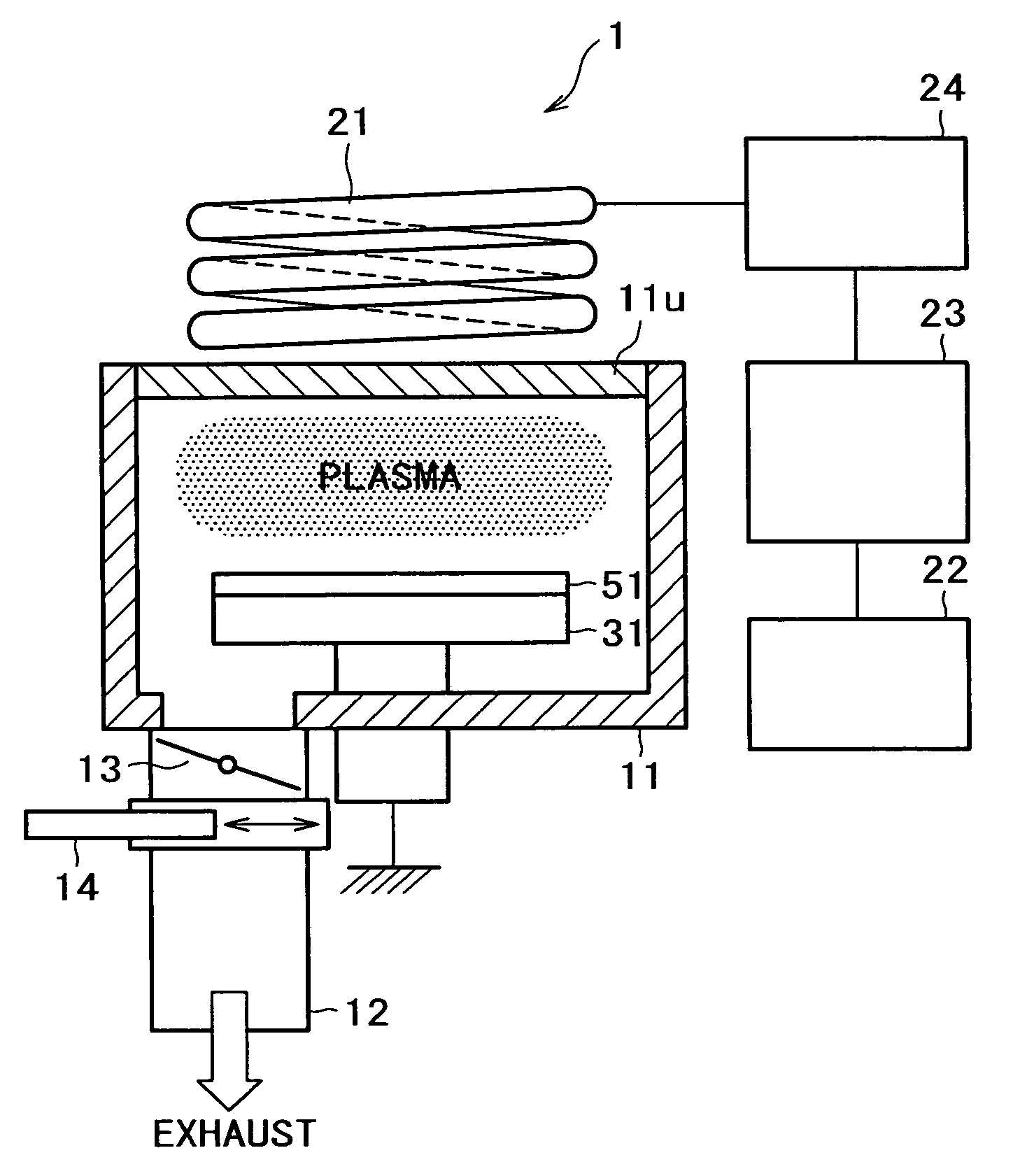
[0039]In the plasma surface treatment system according to the present invention, a high-frequency electric field is for irradiation with a plasma undergoing pulse modulation in the range of not more than 70 μsec, for example. The means for exciting the plasma is not particularly limited, inasmuch as the means is for exciting a plasma by use of a high-frequency. Examples of the exciting means include inductively coupled plasma (ICP), microwave, electron cyclotron resonance (ECR), ultra-high frequency (UHF), helicon wave, and capacitive coupling.

[0040]As the material gas for generating nitrogen molecules and atoms in plasma, there may be used not only nitrogen (N2) but also ammonia (NH3), and combination of nitrogen (N2) with hydrogen (H2), helium (He), argon (Ar), xenon (Xe), krypton (Kr) or the like.

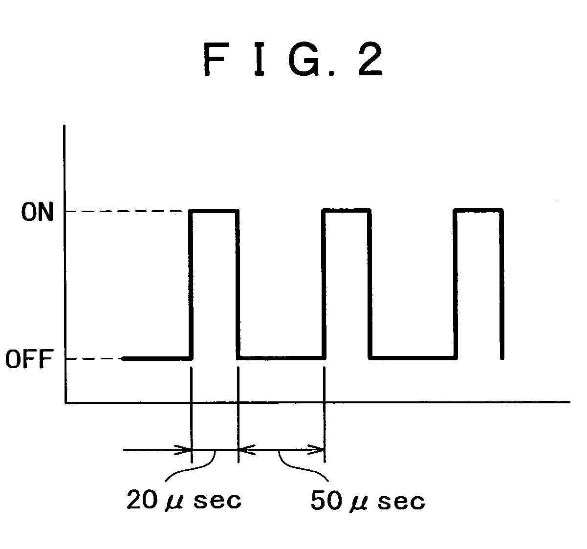
[0041]The pulse modulation of the high-frequency electric field is conducted with a high-frequency electric field application time in the range of from 5 to 50 μsec. If the high-frequenc...


PUM

PropertyMeasurementUnit
Fractionaaaaaaaaaa
Timeaaaaaaaaaa
Ratioaaaaaaaaaa

Abstract

A plasma surface treatment system for irradiating a surface of a substrate to be treated with a nitrogen plasma excited by a high-frequency electric field to introduce nitrogen into the surface of the substrate comprises a pulse modulator for pulse modulation of the high-frequency electric field. By applying the high-frequency electric field in a pulsed form, it is possible to realize a nitriding by which the peak of nitrogen concentration is located at a shallower position and a desired nitrogen concentration can be obtained.

Description

RELATED APPLICATION DATA[0001]The present application claims priority to Japanese Application(s) No(s). P2003-084568 filed Mar. 26, 2003, which application(s) is / are incorporated herein by reference to the extent permitted by law.BACKGROUND OF THE INVENTION[0002]The present invention relates to a plasma surface treatment system and a plasma surface treatment method, and particularly to a plasma surface treatment system and a plasma surface treatment method for introducing nitrogen into a surface of a substrate to be treated which is for use in production of a semiconductor device and which is provided with a silicon oxide film, a metallic oxide film or the like on the surface thereof.[0003]MOS type silicon semiconductor devices have the problems as to scattering of the threshold voltage and as to suppression of the short channel effect, attendant on miniaturization of transistor structure. As a countermeasure against the problems, there have been developed surface channel type CMOS ...

Claims


Application Information

Patent Timeline
IPC IPC(8): H01L21/469C23C14/32H01L21/31H01J37/32H01L21/28H01L21/306H01L21/314
CPCH01J37/321H01L21/3144H01L21/28202H01L21/28185H01L21/306H01L21/0234H01L21/02332
Inventor FUKUDA, SEIICHISAMUKAWA, SEIJI
Owner SONY CORP
Why Eureka
Try Eureka