Method for manufacturing semiconductor thin film

Active Publication Date: 2006-03-07
PANASONIC CORP
View PDF2 Cites 7 Cited by
  • Summary
  • Abstract
  • Description
  • Claims
  • Application Information

AI Technical Summary

Benefits of technology

[0007]A conventional method for manufacturing a semiconductor thin film using the ELO method will now be described.
[0008]FIG. 25A and FIG. 25B are cross-sectional views sequentially illustrating steps in the conventional method for manufacturing a semiconductor thin film.
[0009]First, as illustrated in FIG. 25A, a first semiconductor layer 102 made of gallium nitride (GaN) and having a thickness of about 1 μm is grown as a base layer on a substrate 101 made of sapphire by a metal organic chemical vapor deposition (MOCVD) method, for example. Then, a mask-forming film made of silicon oxide (SiO2) and having a thickness of about 200 μm is deposited on the first semiconductor layer 102 by a chemical vapor deposition (CVD) method, for example. Then, a resist pattern having a planar stripe pattern (not shown) is formed on the mask-forming film by a photolithography method, and then the mask-forming film is wet-etched with hydrogen fluoride using the formed resist pattern as a mask, thereby forming, from the mask-forming film, a mask film 103 having a stripe pattern.
[0010]Next, as illustrated in FIG. 25B, a second semiconductor layer 104 having a thickness of about 100 μm is re-grown (through an ELO process) on the first semiconductor layer 102 with the mask film 103 formed thereon by a hydride vapor phase epitaxy (HVPE) method. In this process, gallium chloride (GaCl), which is a group III source obtained by reacting metal gallium (Ga) with a hydrogen chloride (HCl) gas, and ammonia, which is a nitrogen source, are used as material gases. With the HVPE method, the growth of the second semiconductor layer 104 made of gallium ni

Problems solved by technology

Thus, further reducing the defect density in the second semiconductor layer 104 requires high-precision tools, thereby increasing the manufacturing cost.
Moreover, it is not possible to obtain openings of a size below the lower limit, which is dictated by the level of the state-of-the-art microprocessing technology.
Moreover, when the thickness of the second semiconduc

Method used


Image

  • Method for manufacturing semiconductor thin film
  • Method for manufacturing semiconductor thin film
  • Method for manufacturing semiconductor thin film

Examples


first embodiment

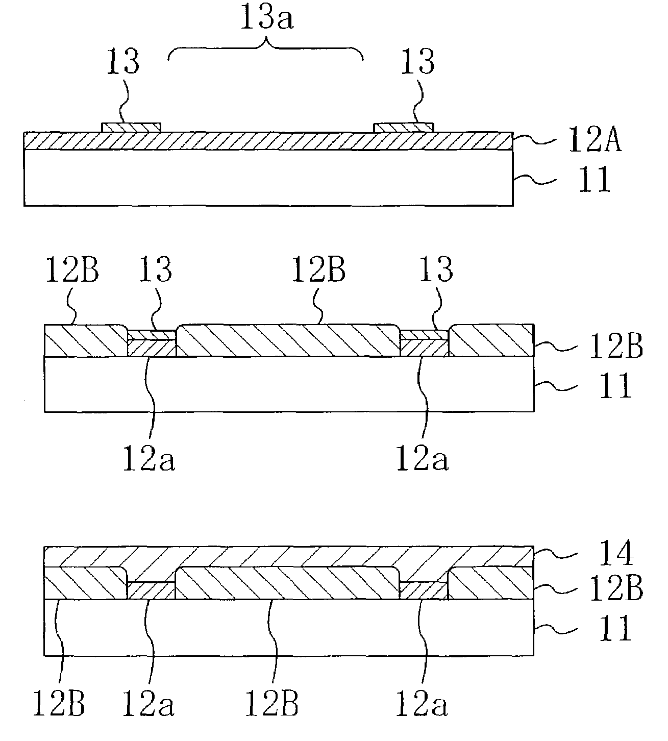
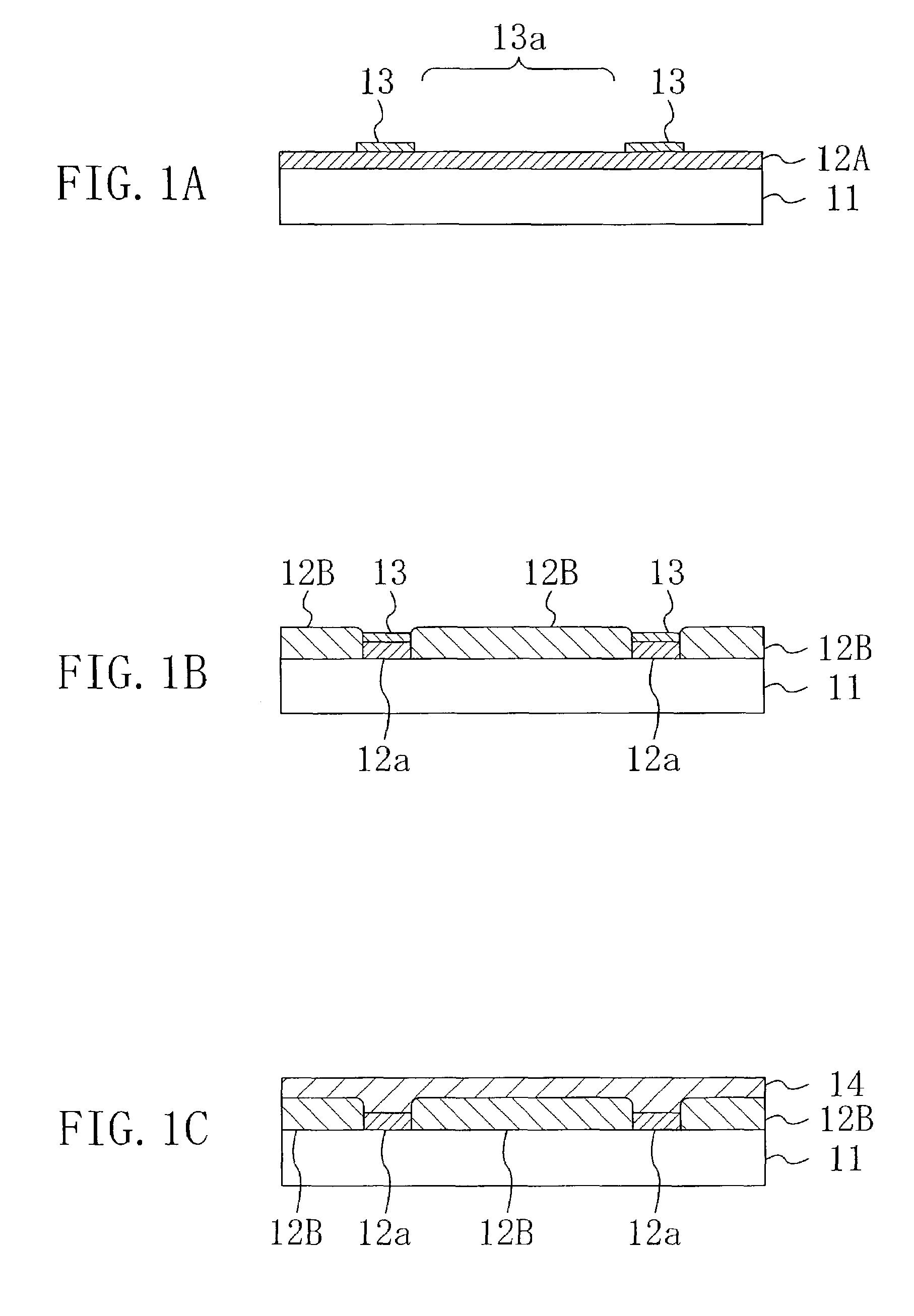
[0116]The first embodiment of the present invention will now be described with reference to the drawings.

[0117]FIG. 1A to FIG. 1C are cross-sectional views sequentially illustrating steps in a method for manufacturing a semiconductor thin film according to the first embodiment of the present invention.

[0118]As illustrated in FIG. 1A, first, a first semiconductor layer 12A made of gallium nitride (GaN) and having a thickness of about 1 μm is grown on the principal surface of a sapphire (single-crystal Al2O3) substrate 11 by a metal organic chemical vapor deposition (MOCVD) method, for example, using trimethylgallium (TMGa) as a group III source and ammonia (NH3) as a nitrogen source. Herein, a so-called a low-temperature buffer layer may be provided between the substrate 11 and the first semiconductor layer 12A for relieving the lattice mismatch between the substrate 11 and the nitride semiconductor grown on the substrate 11. For example, the low-temperature buffer layer is made of a...

second embodiment

[0134]The second embodiment of the present invention will now be described with reference to the drawings.

[0135]FIG. 4A to FIG. 4D and FIG. 5A and FIG. 5B are cross-sectional views sequentially illustrating steps in a method for manufacturing a semiconductor thin film according to the second embodiment of the present invention.

[0136]First, as illustrated in FIG. 4A, the first semiconductor layer 12A made of gallium nitride and having a thickness of about 1 μm is grown on the principal surface of the substrate 11 made of sapphire by an MOCVD method using trimethylgallium as a group III source and ammonia as a nitrogen source. Again, a low-temperature buffer layer may be provided between the substrate 11 and the first semiconductor layer 12A.

[0137]Then, a mask-forming film made of silicon and having a thickness of about 100 nm is deposited on the first semiconductor layer 12A by, for example, a CVD method in which monosilane is decomposed. Then, a resist pattern having a planar stripe...

third embodiment

[0150]The third embodiment of the present invention will now be described with reference to the drawings.

[0151]FIG. 6A to FIG. 6E are cross-sectional views sequentially illustrating steps in a method for manufacturing a semiconductor thin film according to the third embodiment of the present invention.

[0152]First, as illustrated in FIG. 6A, the first semiconductor layer 12A made of gallium nitride and having a thickness of about 1 μm is grown on the principal surface of the substrate 11 made of sapphire by an MOCVD method using trimethylgallium as a group III source and ammonia as a nitrogen source. Again, a low-temperature buffer layer may be provided between the substrate 11 and the first semiconductor layer 12A.

[0153]Then, a mask-forming film made of silicon and having a thickness of about 100 nm is deposited on the first semiconductor layer 12A by, for example, a CVD method in which monosilane is decomposed. Then, a resist pattern having a planar stripe pattern (not shown), for ...


PUM


Abstract

A substrate with a second semiconductor layer and a second mask film formed thereon is subjected to a heat treatment in an oxidizing atmosphere. Thus, second oxidized regions are formed through oxidization of the second semiconductor layer in regions of the second semiconductor layer that are not covered by the second mask film. At the same time, a second base layer is formed in each region that is interposed by the second oxidized regions. Then, the second mask film is removed, and a third semiconductor layer is selectively grown on the surface of the second base layer that is exposed between the second oxidized regions so as to cover the second oxidized regions, after which the first oxidized regions and the second oxidized regions covering the entire upper surface of the substrate are removed.

Description

BACKGROUND OF THE INVENTION[0001]The present invention relates to a method for manufacturing a semiconductor thin film that can be used in short-wavelength light emitting diode devices, short-wavelength semiconductor laser devices and high-speed electronic devices.[0002]A group III–V nitride semiconductor material, having a wide forbidden band, can be used in various light emitting devices, such as light emitting diode devices and short-wavelength semiconductor laser devices that are capable of emitting light of a color in a visible region such as blue, green or white. For its high electron saturated drift velocity, in addition to the wide forbidden band, it is also a promising material for electronic devices such as high-frequency devices and high-power devices.[0003]Among others, light emitting diode devices using a nitride semiconductor have already been in practical use in large-size display apparatuses, traffic signals, etc. Particularly, white light emitting diode devices, whi...

Claims


Application Information

Patent Timeline
IPC IPC(8): H01L21/8242H01L21/20H01L21/762
CPCH01L21/76251H01L21/0237H01L21/02381H01L21/0242H01L21/02639H01L21/0254H01L21/02546H01L21/0262H01L21/02532
Inventor UEDA, TETSUZONAKAYAMA, HISASHIYURI, MASAAKI
Owner PANASONIC CORP
Why Eureka
Try Eureka