Method of forming trench transistor with chained implanted body including a plurality of implantation with different energies

a technology of trench transistors and implanted bodies, applied in the direction of diodes, semiconductor devices, electrical apparatus, etc., can solve the problems of difficult to achieve in practice, extremely low on-resistance, and broken handling

Inactive Publication Date: 2006-05-30
ADVANCED ANALOGIC TECHNOLOGIES INCORPORATED
View PDF27 Cites 30 Cited by
  • Summary
  • Abstract
  • Description
  • Claims
  • Application Information

AI Technical Summary

Benefits of technology

[0048]These problems are solved in a super self-aligned (SSA) trench DMOSFET in accordance with this invention. An SSA trench MOSFET according to this invention comprises a semiconductor body having a trench formed therein, a wall of the trench intersecting a major surface of the semiconductor body at a trench corner. The semiconductor body comprises a source region of a first conductivity type adjacent the trench and the major surface of the semiconductor body; a body region of a second conductivity type forming a junction with the source region, the body region comprising a channel region adjacent a wall of the trench; and a drain region of the first conductivity type forming a junction with the body region. A gate is disposed in the trench. A gate oxide layer borders the gate. The gate oxide layer includes a first portion adjacent the channel region and a second portion overlying the gate, the first portion being thicker than the second portion. A metal layer is in contact with the major surface of the semiconductor body, and the contact between the metal layer and the major surface extends laterally to the trench corner. The first portion of the gate oxide layer prevents shorting between the gate and the source, thereby allowing the contact between the metal layer and the major surface to extend to the corner of the trench. Thus, with the contact being “self-aligned” to the trench without the risk of a gate-source short, the design rules discussed above can be avoided, and the width of the mesa between segments of the trench can be made smaller than was possible with conventional MOSFETs. As explained above, this in turn allows the cell density to be increased and the figure of merit A / W to be reduced.
[0049]According to another aspect of the invention, the gate oxide layer also comprises a third portion adjacent the bottom of the trench, the third portion being thicker than the first portion. This reduces the gate-drain capacitance and avoids field plate induced breakdown.
[0050]According to another aspect of the invention, a heavily-doped buried layer, patterned to conform generally to the shape of the trench gate, is used to reduce the on-resistance of the DMOSFET. One way of achieving this structure is to implant the buried layer after the trenches have been formed.
[0052]According to another aspect of this invention, the polysilicon gate filling the trench is deposited in two polysilicon layers. The first polysilicon layer does not cover the mesas, thereby enabling easy ion implantation of the mesas after the formation of the trench.
[0055]According to still another aspect of this invention, in the event that a contact mask with a small feature is employed, the contact may be planarized with a metal such as tungsten to avoid step coverage problems.
[0056]In the prior art, separate masks were typically used to define the trench and the source-metal contact, respectively. This led to the problems of alignment discussed above. According to the process of this invention, the same mask is used to define both the trench and the source-metal contact. The trench is “self-aligned” to the source-metal contact, and the thick oxide layer overlying the gate prevents shorts between the gate and the source.

Problems solved by technology

1. The metal resistance is minimized through the use of a thicker metal layer.
2. Grinding the wafer to the thinnest possible dimension minimizes the substrate resistance. The grinding must be performed near the end of the fabrication process so that the risk of breakage from handling is minimized.
3. There is an unavoidable tradeoff between the avalanche breakdown voltage and the on-resistance of the device. Higher breakdown voltages require thicker, more lightly doped epitaxial layers contributing higher epitaxial resistances. Generally, the doping of the epitaxial layer is chosen so as to provide the most highly-doped layer capable of supporting the required off-state blocking voltage (i.e., its specified avalanche breakdown voltage).
4. The channel resistance is minimized by maximizing the channel perimeter for a given area. The individual cells of the MOSFET may be constructed in any striped or polygonal shape. Ideally, the shape chosen should be one that can be repeated at a regular pitch so that more cells can be connected in parallel in a given area. Paralleling many cells and operating them in tandem can achieve an extremely low on-resistance.
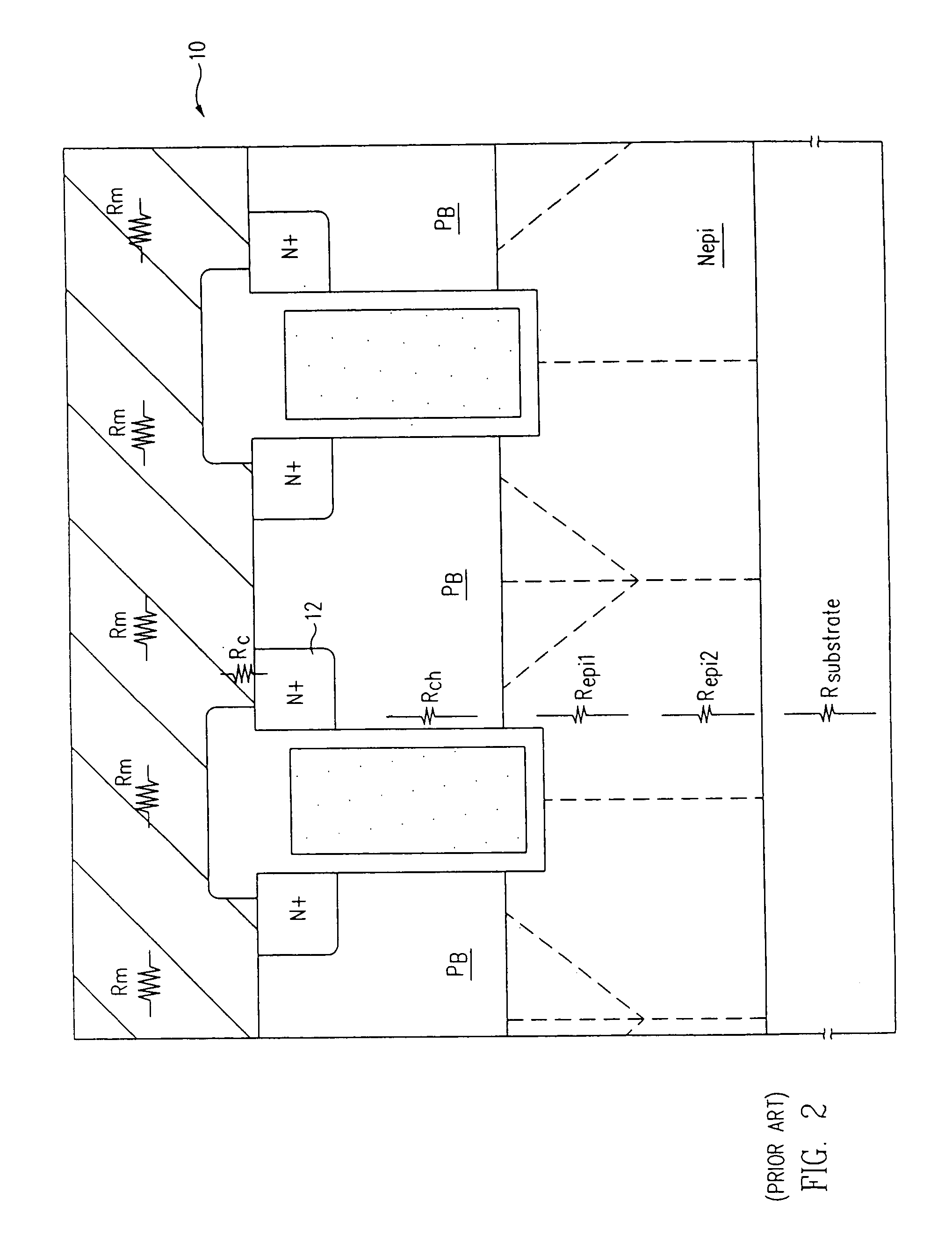
5. Higher cell densities have the advantage that the current in the epitaxial drain becomes uniform closer to the surface, more fully utilizing the epitaxial layer for conduction and reducing the spreading resistance term (Repi1) of the epitaxial resistance. As may be seen be by comparing FIG. 3A with FIG. 3B, a smaller cell pitch reduces the area wasted where no current flows, conducting current uniformly through a greater percentage of the total thickness of the epitaxial layer. The more uniform conducting epitaxial layer exhibits a lower drain resistance.
This circumstance is difficult to achieve in practice, especially in narrow trench gate designs where the alignment tolerances needed to form the source and body regions and to establish a contact to them leads to a wide mesa.
The presence of a source at the square corners in an array of trench-gated DMOS cells has been found to lead to off-state leakage in the device, possibly due to defects along the trench corners or some enhanced diffusion of the source along the corners.
Unfortunately, this corner block feature reduces the gate perimeter of the device and increases channel resistance.
Furthermore, as the cell is scaled to smaller dimensions it becomes impractical to continue to employ the corner block concept since the corners become too close together.
The reduction of source perimeter becomes substantial in such a case and the contact area of the source also suffers.
Despite some claims to the contrary in commercial and industry trade magazines, the packing density of hexagonal cells is no better then the conventional square cell design, resulting in exactly the same A / W.
As photomasking equipment now used exclusively for microprocessor and DRAM manufacturing becomes available for power semiconductor production, the trench width SLD is likely to shrink.
Below a mesa width of around 0.9 to 1.1 μm, even fine line contacts and accurate layer-to-layer alignments become difficult.
Moreover, at these dimensions, other manufacturing-related problems exist.
Many commercial power MOSFETs today are inadequate in this regard and suffer from snapback and ruggedness problems as a result.
Whenever a small contact feature is used to achieve a small mesa and high cell density, another problem occurs with respect to the step coverage of the metal contact.
But the resistance of a thin metal layer, especially under 1.2 μm thick, is too high to be useful in a power device.
Since all of the current must flow through the thin metal and over the step, the device still exhibits high metal resistance and also suffers from poor electromigration performance, despite the thick metal deposition.
The oxide step height in the active contact area can be reduced by depositing a thinner interlayer dielectric (ILD), but the thinner dielectric may exhibit metal breakage wherever metal runs over the polysilicon gate bus.
The thinner ILD also can cause shorts between the source metal and the polysilicon gate bus or lead to a thin oxide sensitive to ESD damage.
The metal step coverage problem occurs anywhere in the die where the source metal crosses the polysilicon gate bus, because the surface polysilicon is too thick.
The thick polysilicon also limits the possible manufacturing process sequence because the polysilicon is too thick to introduce dopants through it.
To summarize, one problem with existing conventional trench-gated vertical DMOS devices is that the cell density cannot be increased and the geometric-area-to-gate-perimeter ratio cannot be further reduced to produce improvements in the area efficiency of low-on-resistance switches, since the construction of conventional trench-gated vertical DMOS imposes fundamental restrictions in cell dimensions.
The resistance penalty is especially significant for low voltage devices where a large portion of the total resistance is attributable to the resistance of the MOS channel (Rch).
The limitations on cell density are primarily a consequence of the minimum width of the mesa between trenches.
Stripe geometries reduce or eliminate the need for frequent or large area abutting source / body shorts, allowing tighter cell pitches but potentially creating problems in achieving good breakdown and snapback characteristics.
But without pushing the design rules to the point where the width of the mesa equals the width of the gate trench, the A / W of the stripe geometry is inferior to the A / W of a square cell geometry having a similar cell pitch.

Method used


Image

  • Method of forming trench transistor with chained implanted body including a plurality of implantation with different energies
  • Method of forming trench transistor with chained implanted body including a plurality of implantation with different energies
  • Method of forming trench transistor with chained implanted body including a plurality of implantation with different energies

Examples


Embodiment Construction

[0095]FIGS. 10A and 10B illustrate the advantages in cell density that can be obtained by reducing the width of the source / body mesa and the cell pitch.

[0096]FIG. 10A illustrates a plot of the mesa dimension YSB against the equivalent cell density for trench gate drawn surface dimensions YG of 1.0, 0.8, and 0.5 μm. The density is plotted both in Mcells / in2 (left axis) and Mcells / cm2 (right axis) from the equation

[0097]D=1(YG+YSB)2·108⁢⁢µm2cm2·Mcells106(23)

[0098]The plot is divided into three regions:

[0099]Region III for YSB>2 μm, where normal butting source-body contacts may be used. The limit in cell densities for this type of device ranges from 67 to 100 Mcells / in2, although 30 to 40 Mcells / in2 densities are the highest in production.

[0100]Region II for 0.9 μmSB2 range, but only provided certain design and manufacturing related problems are overcome (the solutions for which are described later herein).

[0101]Region I for YSB<0.9 μm, where a new technique is required to form the con...


PUM


Abstract

A “chained implant” technique forms a body region in a trench gated transistor. In one embodiment, a succession of “chained” implants can be performed at the same dose but different energies. In other embodiments different doses and energies can be used, and particularly, more than one dose can be used in a single device. This process produces a uniform body doping concentration and a steeper concentration gradient (at the body-drain junction), with a higher total body charge for a given threshold voltage, thereby reducing the vulnerability of the device to punchthrough breakdown. Additionally, the source-body junction does not, to a first order, affect the threshold voltage of the device, as it does in DMOS devices formed with conventional diffused body processes.

Description

CROSS-REFERENCE TO RELATED PATENT APPLICATIONS[0001]This is a divisional and claims the priority of U.S. patent application Ser. No. 10 / 146,668, filed on May 14, 2002, now U.S. Pat. No. 6,750,507, which is a divisional of U.S. patent application No. 09 / 296,959, filed on Apr. 22, 1999, now U.S. Pat. No. 6,413,822, which is hereby incorporated by reference in its entirety.BACKGROUND[0002]FIG. 1 illustrates a conventional vertical double-diffused MOSFET (DMOS) 10 with a trench gate 11, a diffused P-type body diffusion (PB), a shallow N+ source region 12, a P+ body contact region 13, formed in an N-type epitaxial layer Nepi grown on an N+ substrate. A source metal 14, using a butting contact structure, shorts the source and body contact regions 12 and 13. The gate 11 is embedded in a trench 15 etched into the epitaxial layer Nepi, oxidized and then filled with doped polysilicon. The channel of the device is formed along the sidewall of the trench in the silicon region extending between ...

Claims


Application Information

Patent Timeline
Patent Type & Authority Patents(United States)
IPC IPC(8): H01L21/336H01L21/425H01L29/41H01L27/02H01L27/04H01L29/06H01L29/08H01L29/10H01L29/40H01L29/423H01L29/45H01L29/739H01L29/78
CPCH01L27/0255H01L29/7813H01L29/7808H01L29/7811H01L29/0696H01L29/0878H01L29/1095H01L29/42368H01L29/456H01L29/407H01L29/76
Inventor WILLIAMS, RICHARD K.GRABOWSKI, WAYNE
Owner ADVANCED ANALOGIC TECHNOLOGIES INCORPORATED
Why Eureka
Try Eureka