Method of manufacturing semiconductor devices

a manufacturing method and semiconductor technology, applied in the direction of semiconductor/solid-state device testing/measurement, instruments, nuclear elements, etc., can solve the problems of complex devices, difficult to ship the needed semiconductor devices stably within an acceptable time period, and low yield rate, so as to improve the yield of chips. , the effect of stable production of semiconductor devices

Inactive Publication Date: 2006-05-30
LONGITUDE SEMICON S A R L
View PDF21 Cites 19 Cited by
  • Summary
  • Abstract
  • Description
  • Claims
  • Application Information

AI Technical Summary

Benefits of technology

[0050]Thus, according to the present invention, since the position information of a chip of the assembly which is determined to be faulty is analyzed based on the chip data held in that chip, a malfunction of a manufacturing device or a processing step which may cause failures in the semiconductor devices in the wafer process can be identified quickly. Furthermore, the cause of a failure can be determined accurately from the information giving the position of wafer in a lot and the position of a chip on the wafer, so that an abnormal manufacturing device or processing step can be corrected quickly and the yield of chips can be improved rapidly

Problems solved by technology

In general, the manufacturing devices are complicated in their construction and include many factors causing the yield rate to be lowered.
Thus, unless the development of the processing steps necessary for the high-degree integration of circuits and the stabilization of such processing steps have been completed as quickly as possible, it is quite difficult to ship the needed semiconductor devices stably within an acceptable time period.
However, since there are several tens of manufacturing devices and hundreds of processing steps involved in the manufacture of one semiconductor device, a big problem is how to quickly find in which manufacturing device or in which processing step the failure occurred.
In such a case, it will be assumed that the cause of failures may exist in an immersion wet etching process where a resist or an oxide film was removed.
The reason for this is that the electric field may be uneven in the peripheral area in such a device.
In this case, however, it is not possible to perform a high-speed test of operation in a wafer state due to the facts that the probe has parasitic capacitance and that it is not possible to provide in the time available a wafer tester possessing a speed comparable to the enhanced speed of semiconductor devices.
Also, it is inefficient to perform, in a wafer state, tests about special items such as a breakdown test in which a high voltage is applied and an environmental test which is carried out at room, low and high temperatures.
In addition, since a plurality of semiconductor devices are formed on the same semiconductor substrate in a wafer state, there is another problem that it is not possible to carry out a test on such items without the possibility that interference with other chips may occur.
Furthermore, a large number of semiconductor devices cannot be tested simultaneously, since control signals and data must be conveyed to input/output pads of semiconductor devices through a limited number of probes.
In other words, the testing of semiconductor devices in a wafer state has a significant disadvantage since the number of semiconductor devices which can be tested simultaneously is limited, and the production efficiency is decreased when the test is performed in relation to many operational and electric characteristics.
The semiconductor devices which are judged to be faulty after assembly is not high in number as compared to the failures in the wafer test, but still exist to a certain degree.
However, once assembled in a package, the assembly no longer contains the information about its position in the wafer and consequently, the detection of faulty processing steps as in the first and the second related art cannot be made.
Thus, the semiconductor devices which have been judged to be non-defective in the wafer state and then sealed in packages

Method used


Image

  • Method of manufacturing semiconductor devices
  • Method of manufacturing semiconductor devices
  • Method of manufacturing semiconductor devices

Examples


first embodiment

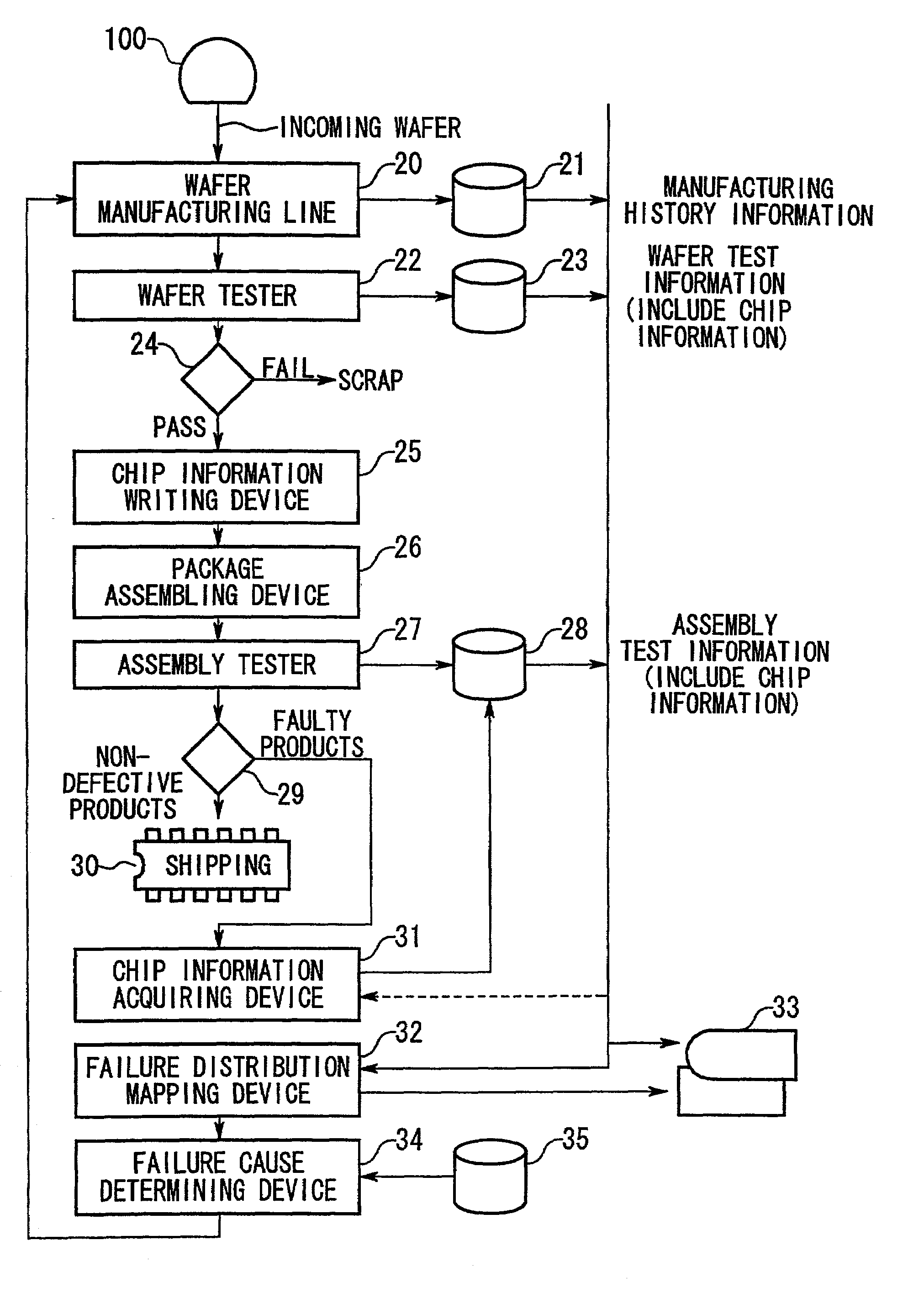
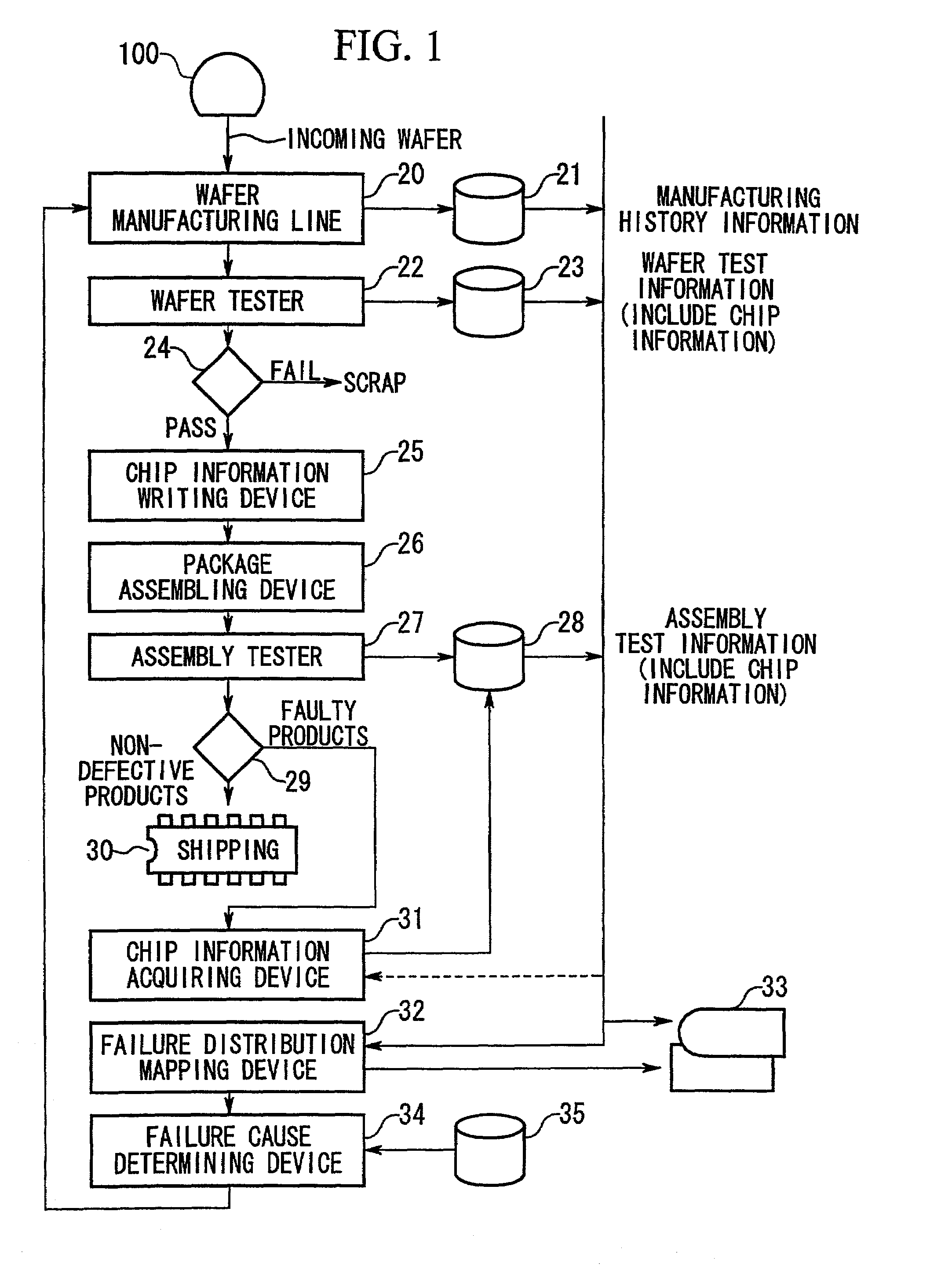
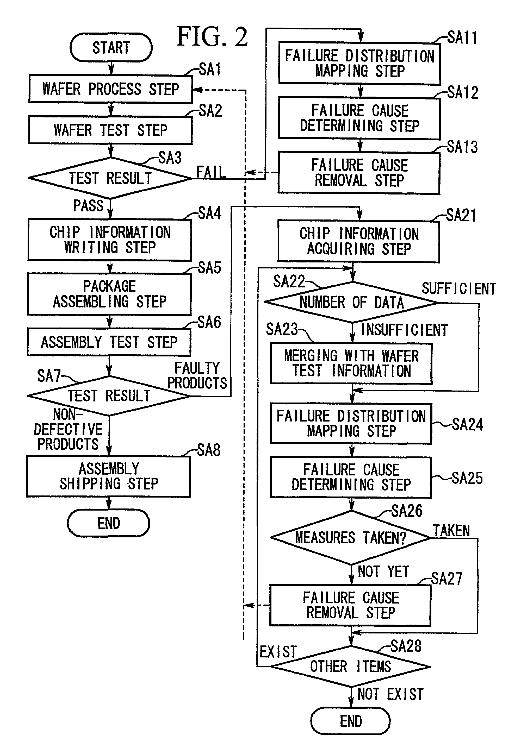
[0079]FIG. 1 is an illustration showing the structure of a semiconductor device manufacturing system in accordance with a first embodiment of the invention, and FIG. 2 is a flow chart which explains the operation of the semiconductor device manufacturing system.

[0080]In FIG. 1, a wafer manufacturing line 20 is constituted by manufacturing devices for performing various semiconductor processes. In a wafer process step SA1 of FIG. 2, transistor elements and wirings are formed in the surface of a wafer 100 to fabricate a semiconductor device. Usually, twenty to fifty sheets of wafer 100 are placed in a carrier and fed as one processing unit (hereinafter referred to as “a lot”) to the wafer manufacturing line 20 to thereby subject them to predetermined wafer processes in predetermined manufacturing devices. Each lot is given a predetermined wafer processing lot number (hereinafter referred to as “a lot number” unless specified otherwise).

[0081]The given lot number is indicated on the ca...

second embodiment

[0115]FIG. 11 shows the structure of a semiconductor device manufacturing system provided in accordance with a second embodiment of the invention, wherein its elements corresponding to those in the first embodiment are designated by like reference numerals and their description will be omitted.

[0116]In the following description, it will be assumed that the semiconductor device to be manufactured is a memory such as a DRAM (dynamic random access memory) which comprises a plurality of memory cells and redundancy circuits which can replace memory cells having defectives (hereinafter referred to as “defective cell”).

[0117]A wafer 100 is fed to a wafer manufacturing line 20 in which the wafer is subjected to predetermined processing steps, as a result of which a plurality of semiconductor memories are formed in the wafer surface.

[0118]Herein, the wafer manufacturing line 20 means a series of processing steps up to the processing step for cutting the wafer into chips and includes all the ...


PUM

PropertyMeasurementUnit
Distributionaaaaaaaaaa

Abstract

A semiconductor device manufacturing system is provided in which chip position information is read without removing resin from a package so that the cause of a failure can be quickly identified and removed and the yield of chips can be rapidly improved. A replacement address reading device reads redundancy addresses from a semiconductor device which is determined as faulty in a test performed after the semiconductor device has been sealed into a package. A chip position analyzing device estimates, from the combination of these redundancy addresses, a lot number, a wafer number and a chip number of the faulty semiconductor device. A failure distribution mapping device maps the distribution of faulty chips in each wafer in the lot based on these numbers thus obtained. A failure cause determining device identifies which manufacturing device or processing step has caused the failures in the wafer process based on the above distribution.

Description

CROSS REFERENCE TO RELATED PATENT APPLICATIONS[0001]This application is a division of U.S. Pat. No. 6,349,240, issued Feb. 9, 2002, and based on Japanese Patent Application No. 2000-87480, filed Mar. 27, 2000, by Sumio OGAWA, Minoru UEKI and Shinichi HARA. This application claims only subject matter disclosed in the parent application and therefore presents no new matter.BACKGROUND OF THE INVENTION[0002]1. Field of the Invention[0003]This invention relates to a semiconductor device manufacturing system for determining the cause of failures in a semiconductor device which has become faulty after the division of a wafer into a plurality of chips, and also to a method of manufacturing semiconductor devices as well as a failure analyzing device.[0004]2. Description of the Related Art[0005]In recent years, the life cycle of electronic devices has been becoming shorter and shorter, and it has become imperative for developers to complete the designs of such electronic devices in a short pe...

Claims


Application Information

Patent Timeline
IPC IPC(8): G06F19/00H01L21/00G11C29/44H01L21/02H01L21/66
CPCH01L22/20H01L2924/0002Y10T29/41H01L2924/00H01L21/00
Inventor OGAWA, SUMIOUEKI, MINORUHARA, SHINICHI
Owner LONGITUDE SEMICON S A R L
Why Eureka
Try Eureka