Long retention time single transistor vertical memory gain cell

a single transistor and vertical memory technology, applied in the field of single transistor vertical memory gain cells, can solve the problems of increasing the operation of the device, and the size of the capacitor, and the degree to which further reduction in size and corresponding increase in the total count and density of the individual devices, etc., to achieve higher saturated electron velocities and breakdown field strengths, higher current densities, and high band gap energy eg

Active Publication Date: 2006-12-19
MICRON TECH INC
View PDF28 Cites 31 Cited by
  • Summary
  • Abstract
  • Description
  • Claims
  • Application Information

AI Technical Summary

Benefits of technology

[0012]Preferred embodiments take advantage of the material properties of silicon carbide as a semiconductor material. Silicon carbide has a significantly higher band gap energy Eg than silicon (3.25 eV vs. 1.12 eV) as well as higher saturated electron velocities and breakdown field strengths. Silicon carbide thus has a rate of thermally generated leakage currents that are practically negligible in silicon carbide as compared to silicon and can provide higher current densities. Preferred embodiments...

Problems solved by technology

However, there are ever-present limitations to the degree to which further reduction in size and corresponding increase in the total count and density of individual devices may be practically realized with current semiconductor processing technologies.
Scaling however can lead to difficulties in operation of the devices as reduction in the size of the capacitor, as well as reduction in operating voltages reduces the available electrical signal output from the memory cells making reliable read/write operations to the memory cells more difficult.
An additional difficulty is that with the reduced physical size and operating voltages attendant to scaling, so-called soft errors can more frequently arise when incident radiation, such as alpha particles, activates charge carriers in the cel...

Method used


Image

  • Long retention time single transistor vertical memory gain cell
  • Long retention time single transistor vertical memory gain cell
  • Long retention time single transistor vertical memory gain cell

Examples


Embodiment Construction

[0031]Reference will now be made to the drawings wherein like reference numerals refer to like structures and materials throughout. It will be understood that the figures are provided for illustrative purposes for the various embodiments described herein and should not be interpreted as being to scale or illustrating precise quantitative or proportional relationships.

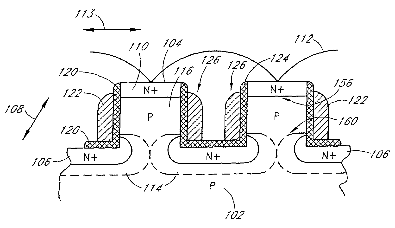
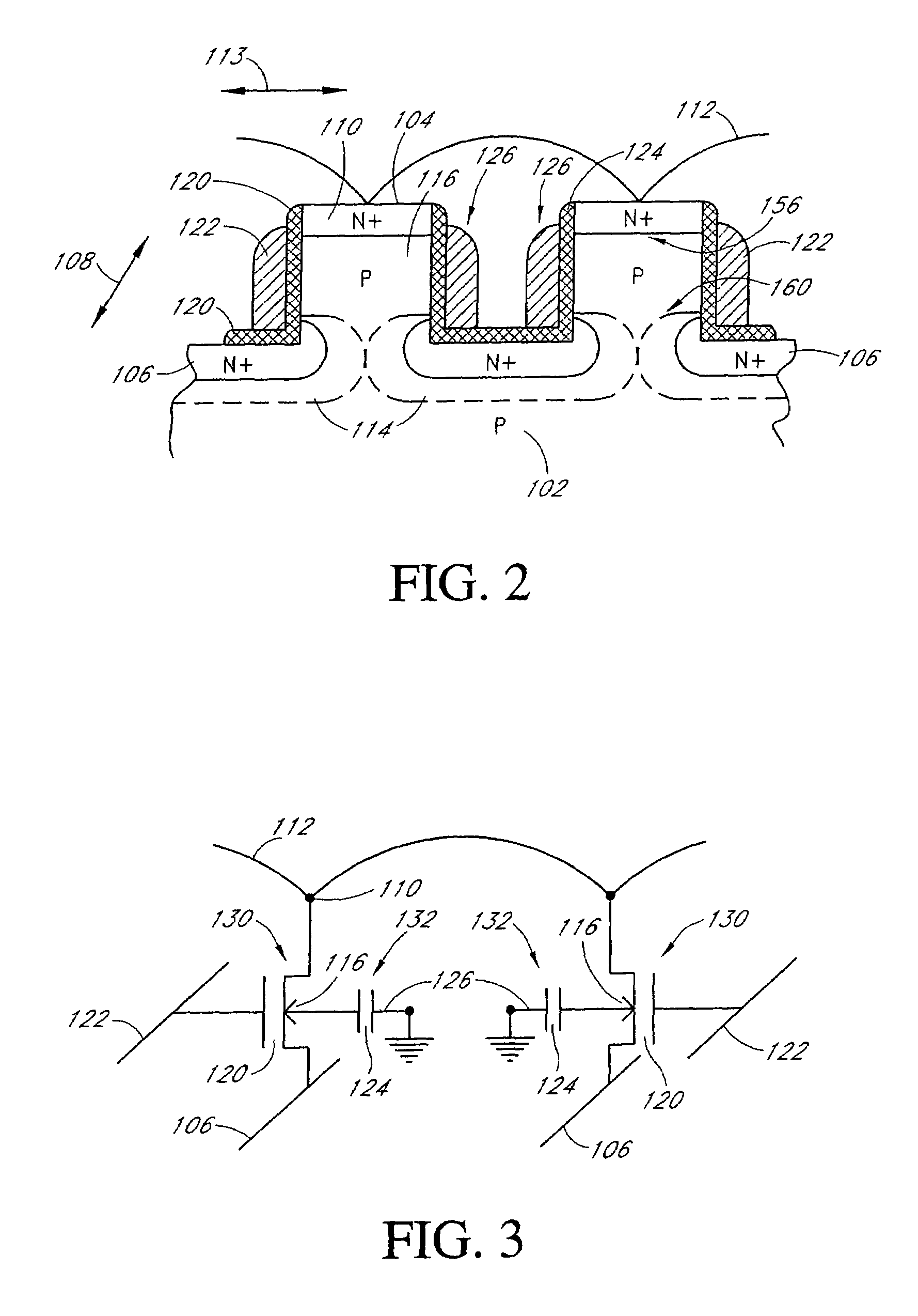
[0032]FIG. 2 illustrates, in cross-sectional view, one embodiment of a single transistor memory gain cell 100. The cell 100 provides a readily fabricatable high-density memory gain cell with relatively long retention times that can facilitate extremely high device densities and is resistant to soft errors, such as from incident alpha particle radiation. The structure, operation of, and fabrication of the cell 100 will be described in this embodiment with analogy to an n-type metal oxide semiconductor (NMOS) transistor for ease of understanding. However, it will be understood that in other embodiments, an analogous compl...


PUM


Abstract

A single transistor vertical memory gain cell with long data retention times. The memory cell is formed from a silicon carbide substrate to take advantage of the higher band gap energy of silicon carbide as compared to silicon. The silicon carbide provides much lower thermally dependent leakage currents which enables significantly longer refresh intervals. In certain applications, the cell is effectively non-volatile provided appropriate gate bias is maintained. N-type source and drain regions are provided along with a pillar vertically extending from a substrate, which are both p-type doped. A floating body region is defined in the pillar which serves as the body of an access transistor as well as a body storage capacitor. The cell provides high volumetric efficiency with corresponding high cell density as well as relatively fast read times.

Description

RELATED APPLICATIONS[0001]This application is a divisional of U.S. patent application Ser. No. 10 / 933,814, filed Sep. 2, 2004, which is incorporated herein in its entirety by reference.BACKGROUND OF THE INVENTION[0002]1. Field of the Invention[0003]The invention relates to the field of semiconductor transistors and more particularly to a single transistor memory gain cell with long retention times.[0004]2. Description of the Related Art[0005]Semiconductor memory devices are widely employed in a wide variety of electronic devices such as consumer electronics, computer systems, etc. The semiconductor memory devices can provide storage capacity for operating software as well as data storage, such as for text files, audio / video files, etc. A popular and commonly employed type of memory is known as dynamic random access memory (DRAM). DRAM provides the advantage of relatively rapid ability to write and read data as well as a relatively simple circuit design which facilitates relatively h...

Claims


Application Information

Patent Timeline
IPC IPC(8): H01L21/8242
CPCH01L27/108H01L27/10802H01L29/7841H01L29/1608H10B12/20H10B12/00
Inventor FORBES, LEONARD
Owner MICRON TECH INC
Why Eureka
Try Eureka