Formulation and fabrication of an improved Ni based composite Ohmic contact to n-SiC for high temperature and high power device applications

a technology of composite ohmic contact and ni based ni, which is applied in the direction of semiconductor devices, basic electric elements, electrical apparatus, etc., can solve the problems of significant challenges to overcome, unreliability of devices, and complex metallization of wide bandgap semiconductors (sic). achieve excellent electrical properties, reduce the effect of metallization complexity

a technology of composite ohmic contact and ni based ni, which is applied in the direction of semiconductor devices, basic electric elements, electrical apparatus, etc., can solve the problems of significant challenges to overcome, unreliability of devices, and complex metallization of wide bandgap semiconductors (sic). achieve excellent electrical properties, reduce the effect of metallization complexity

US7163882B1Inactive Publication Date: 2007-01-16UNITED STATES OF AMERICA THE AS REPRESENTED BY THE SEC OF THE ARMY

Image

  • Formulation and fabrication of an improved Ni based composite Ohmic contact to n-SiC for high temperature and high power device applications
  • Formulation and fabrication of an improved Ni based composite Ohmic contact to n-SiC for high temperature and high power device applications
  • Formulation and fabrication of an improved Ni based composite Ohmic contact to n-SiC for high temperature and high power device applications

Examples


Embodiment Construction

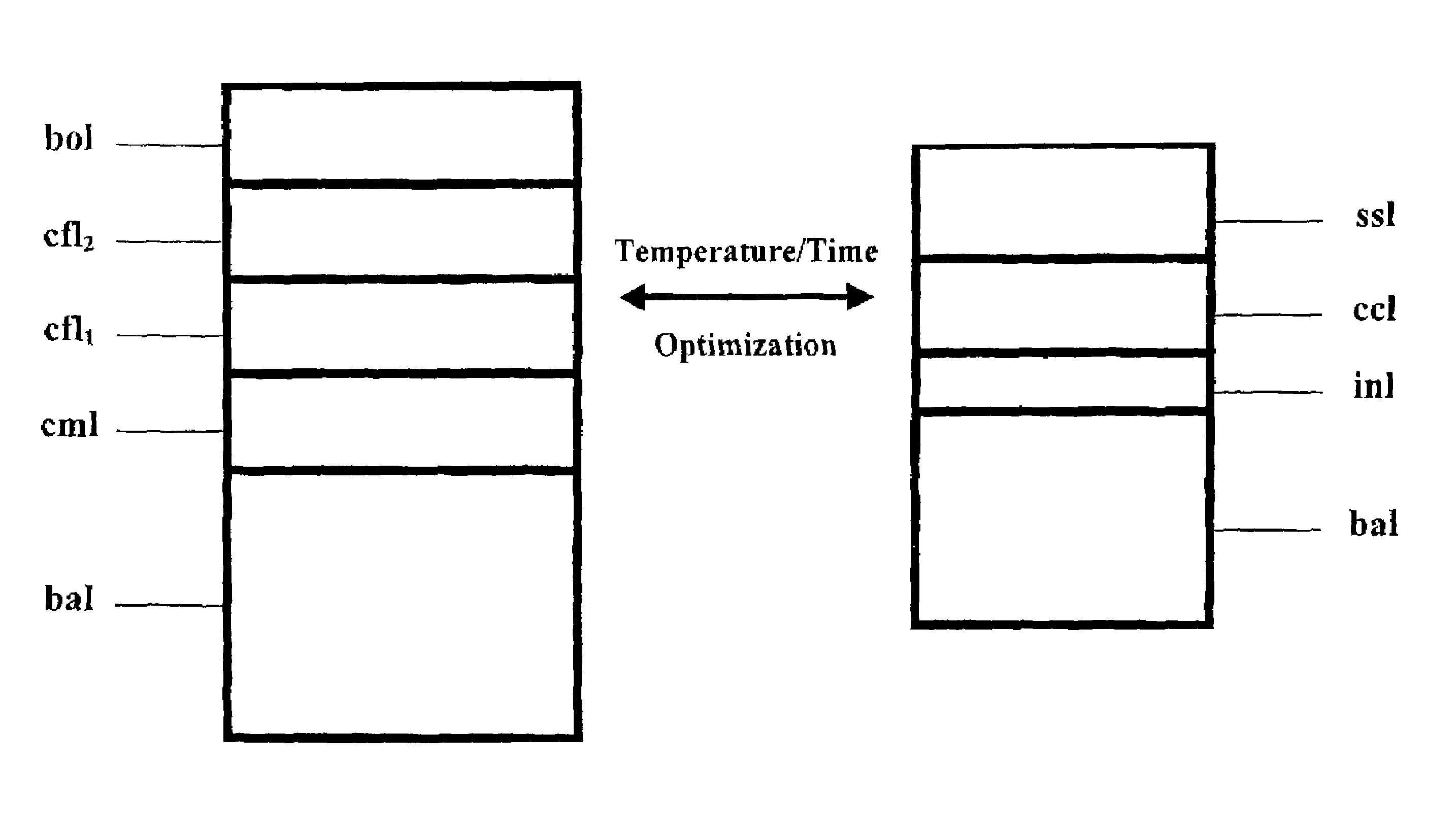
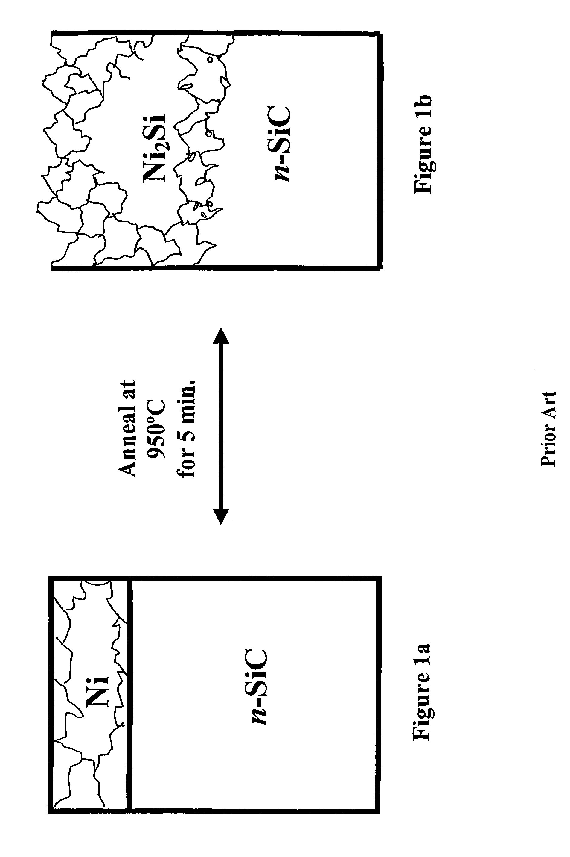
[0056]The present invention overcomes undesirable phenomena associated with annealed pure Ni-nSiC Ohmic contacts. FIGS. 1(a) and 1(b) show schematic representations of prior art pure Ni Ohmic contacts to n-SiC. FIG. 1(a) shows the as-deposited Ni-nSiC and FIG. 1(b) shows the Ni-nSiC Ohmic contact, annealed at 950° C. These contacts are plagued with problems including a rough surface, the presence of unreacted carbon, a broad, non-abrupt interface layer and the presence of Kiirdendall voids.

[0057]The present invention successfully addresses the disadvantages of the prior art by limiting the interfacial reaction, tying up unreacted carbon, limiting contact thickness increase and eliminating voids and surface roughness while maintaining electrical integrity.

[0058]All semiconductor devices require high quality, low resistivity thermally stable reliable n- and p-type Ohmic contacts. Ohmic contacts are essential for the transfer of signals between the SiC device and external circuitry. Th...


PUM

PropertyMeasurementUnit
temperaturesaaaaaaaaaa

Abstract

A composite Pt / Ti / WSi / Ni Ohmic contact has been fabricated by a physical deposition process which uses electron beam evaporation and dc-sputter deposition. The Ni based composite Ohmic contact on n-Sic is rapid thermally annealed (RTA) at 950° C. to 1000° C. for 30 s to provide excellent current-voltage characteristics, an abrupt, void free contact-SiC interface, retention of the as-deposited contact layer width, smooth surface morphology and an absence of residual carbon within the contact layer and / or at the Ohmic contact-SiC interface. The annealed produced Ni2Si interfacial phase is responsible for the superior electrical integrity of the Ohmic contact to n-SiC. The effects of contact delamination due to stress associated with interfacial voiding has been eliminated. Wire bonding failure, non-uniform current flow and SiC polytype alteration due to extreme surface roughness have also been abolished. The Ohmic contact also avoids electrical instability associated with carbon inclusions within the contact metallization and / or at the contact-SiC interface, that occur under prolonged high temperature and power device operations. Overall, this contact is reliable for high temperature and high power operations and the stresses inclusive of use under those conditions.

Description

CROSS-REFERENCE TO RELATED APPLICATIONS[0001]This application is a divisional of application Ser. No. 09 / 939,420, filed Aug. 27, 2001, and now U.S. Pat. No. 6,759,683.STATEMENT OF GOVERNMENT INTEREST[0002]The invention described herein is the property of the United States Government as represented by the Secretary of the Army, US Army Materiel Command.BACKGROUND OF THE INVENTION[0003]1. Field of the Invention[0004]This invention is directed to a semiconductor device manufacturing process. This invention is also directed to a metallization scheme and fabrication process for forming an Ohmic contact on a wide bandgap semiconductor material. This invention is further directed to a metallization scheme and fabrication process for forming a low resistance, thermally stable Ohmic contact on n-type silicon carbide (SiC) using the post-deposition annealed (950° C.–1000° C.) composite metallization scheme Platinum / Titanium / Tungsten silicide / Nickel (Pt / Ti / WSi / Ni)[0005]2. Discussion of Relevan...

Claims


Application Information

Patent Timeline
16 Jan 2007
Publication
US7163882B1
IPC
H01L21/44; H01L21/04; H01L31/0312
CPC
H01L21/0485; Y10S438/931
Inventors
COLE, MELANIE W.; JOSHI, POORAN C.