

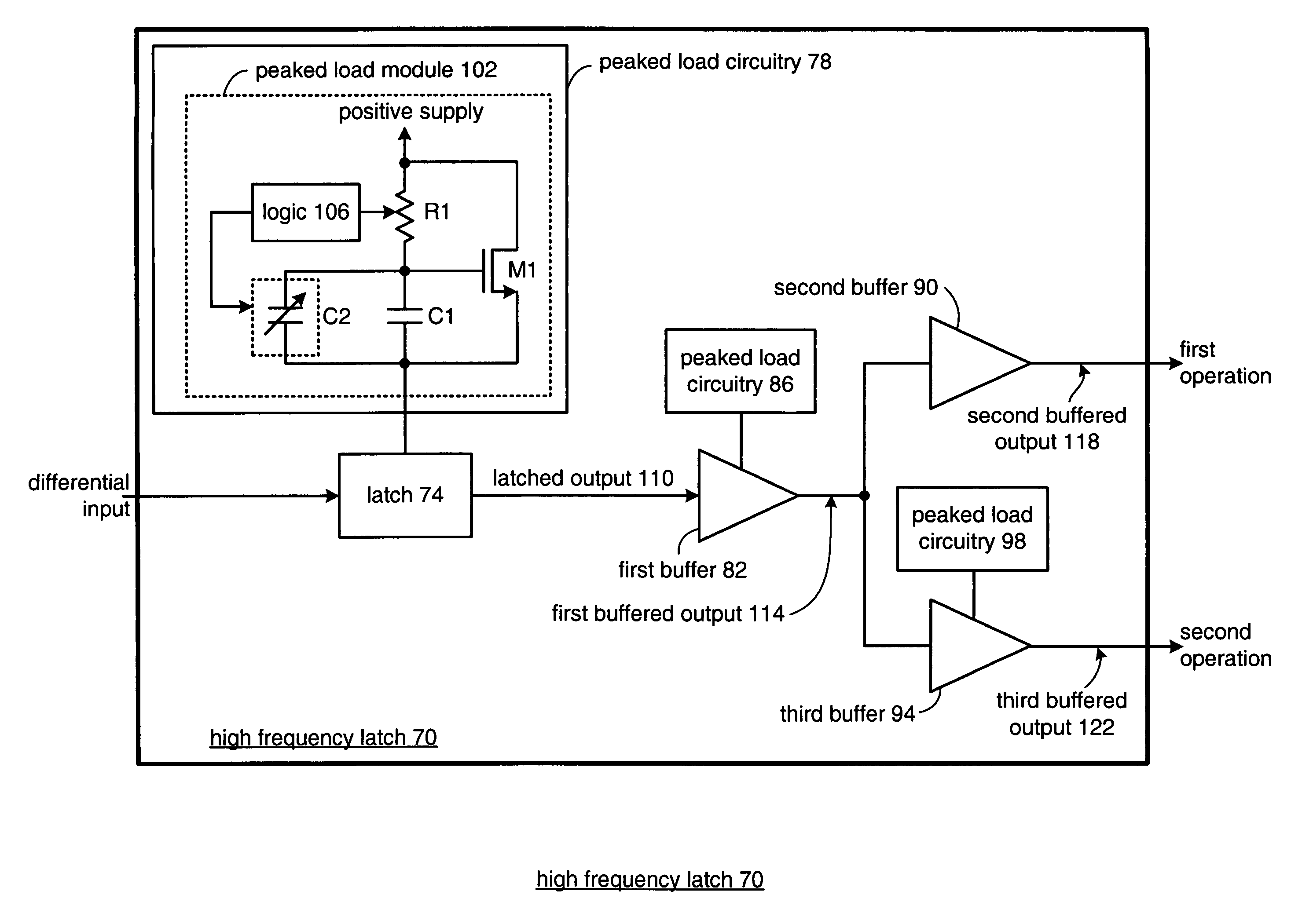
High frequency latch
a latch circuit and high frequency technology, applied in logic circuit coupling/interface arrangement, pulse technique, instruments, etc., can solve the problems of reducing the usefulness limiting the bandwidth of prior art clock recovery circuits, and reducing the high frequency response. , the effect of reducing the coupling
- Summary
- Abstract
- Description
- Claims
- Application Information
AI Technical Summary
Benefits of technology
Problems solved by technology
Method used
Image

Examples
Embodiment Construction
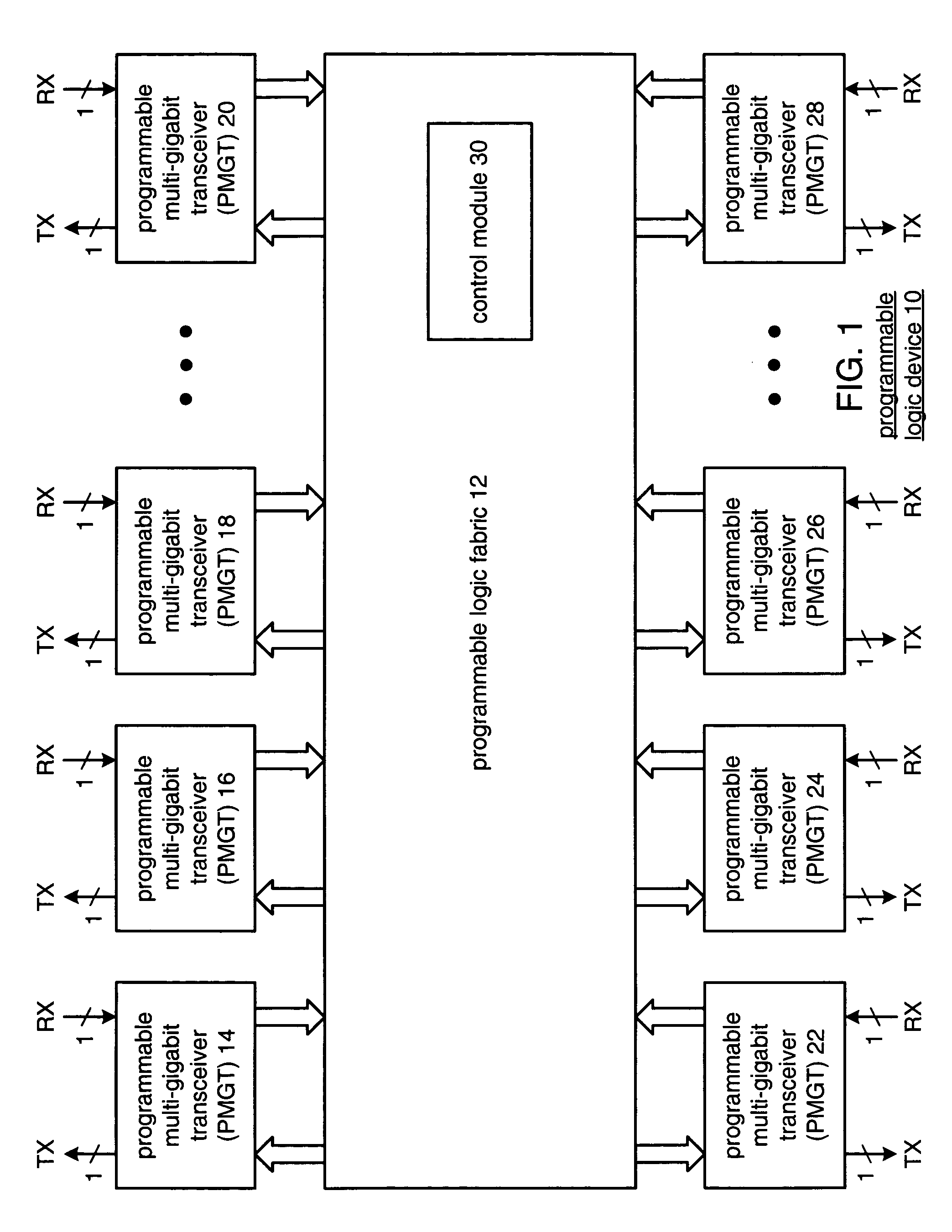
[0025]FIG. 1 is a schematic block diagram of a programmable logic device 10 that includes programmable logic fabric 12, a plurality of programmable multi-gigabit transceivers (PMGTs) 14–28 and a control module 30. The programmable logic device 10 may be a programmable logic array device, a programmable array logic device, an erasable programmable logic device, and / or a field programmable gate array (FPGA). When the programmable logic device 10 comprises a FPGA, the programmable logic fabric 12 may be implemented as a symmetric array configuration, a row-based configuration, a sea-of-gates configuration, and / or a hierarchical programmable logic device configuration. The programmable logic fabric 12 may further include at least one dedicated fixed processor, such as a microprocessor core, to further facilitate the programmable flexibility offered by programmable logic device 10.
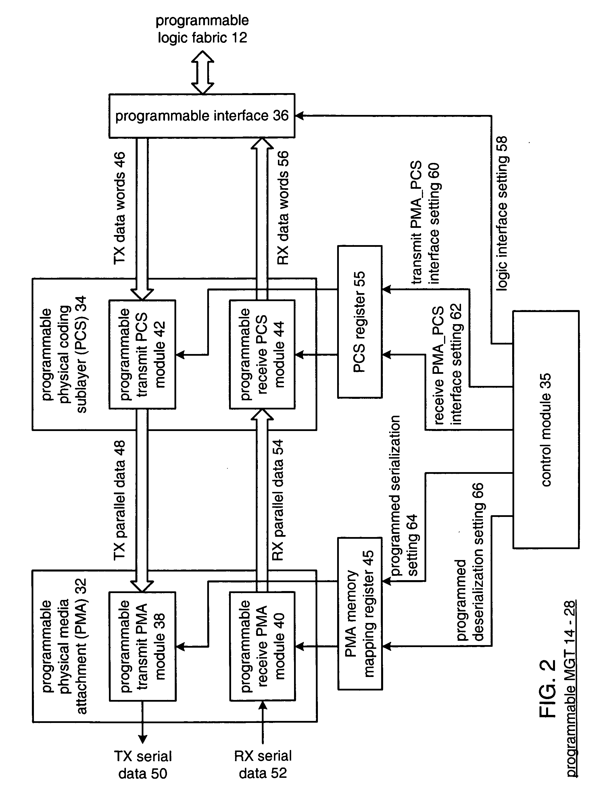
[0026]The control module 30 may be contained within the programmable logic fabric 12 or it may be a separate...
PUM
 Abstract
Description
Claims
Application Information