Semiconductor device and method of fabricating the same

a semiconductor and semiconductor technology, applied in the direction of semiconductor devices, electrical devices, transistors, etc., can solve the problems of difficult to control the position of crystal grain boundaries or crystal orientation, the field effect mobility of tft cannot be made higher than that of a transistor, and the threshold characteristic is improved. , to achieve the effect of small variation in characteristics, high field effect mobility, and improved threshold characteristi

Inactive Publication Date: 2007-07-03
SEMICON ENERGY LAB CO LTD
View PDF68 Cites 50 Cited by
  • Summary
  • Abstract
  • Description
  • Claims
  • Application Information

AI Technical Summary

Benefits of technology

[0015]It is an object of the invention to provide a thin film transistor resolving the above-described problems, in whi

Problems solved by technology

Although in order to increase the field effect mobility of TFT, carriers may be moved smoothly by a channel without being scattered, in the case of TFT using a crystalline silicon film currently reduced to practice, there are many grain boundaries in the channel and therefore, the field effect mobility of TFT cannot be made higher than that of a transistor using a silicon wafer.
Further, although it is known that easiness of flowing carriers in a semiconductor differs also by crystal orientation, according to the conventional crystallizing technology, it is very difficult to align crystal orientation in the direction of carriers flowing in the channel.
According to the above-described conventional crystallizing technology, crystals grow with crystal nuclei accidentally produced in an amorphous silicon film as seeds and therefore, the crystal grain boundaries cannot be eliminated at all, further, it is very difficult to control positions of crystal grain boundaries or crystal orientation.
However, in the case of crystallization by solid phase growth using a heating furnace or the like, when the film thickness is thinned, there is a case that it is difficult to increase a crystal grain size.
Further, also in the case of crystallization by continuous wave laser beam such as YAG laser or pulse laser beam such as excime

Method used


Image

  • Semiconductor device and method of fabricating the same
  • Semiconductor device and method of fabricating the same
  • Semiconductor device and method of fabricating the same

Examples


embodiment 1

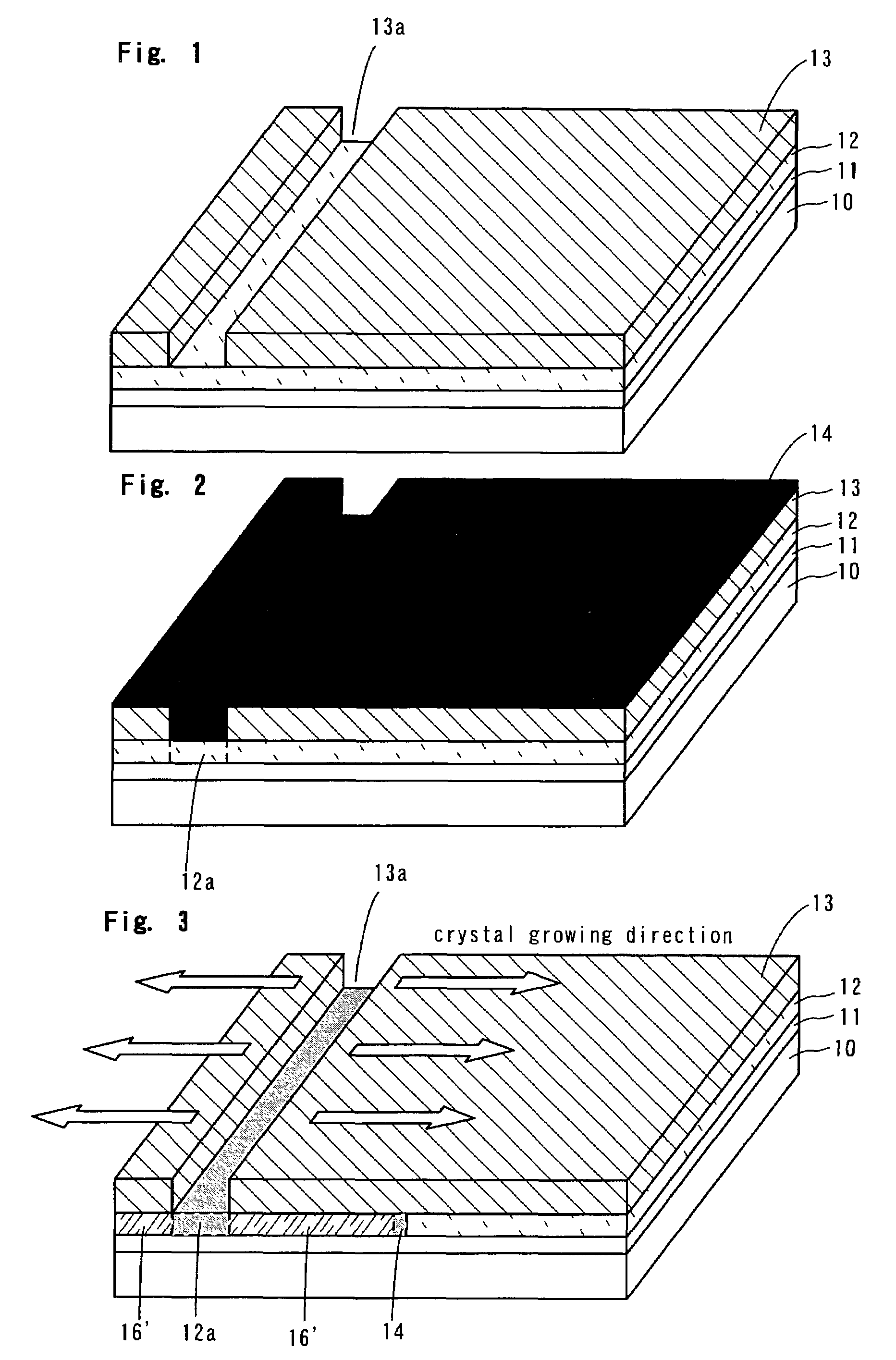
[0105]According to the embodiment, an explanation will be given of an example of a method of forming a first crystalline semiconductor layer by selectively adding a metal element for promoting crystallization to a first amorphous semiconductor film. According to the embodiment, an explanation will be given of using nickel (Ni) and using a solution as a method of adding the metal element.

[0106]Refer to FIG. 1

[0107]There is prepared a substrate 10 for forming a crystalline semiconductor layer. As the substrate 10, a substrate comprising glass of barium boro-silicate glass or aluminum boro-silicate glass, or a substrate comprising quartz or silicon wafer can pertinently be selected in accordance with use of a semiconductor device or process conditions of temperature and the like. A substrate comprising a plastic material having high heat resistance of, for example, polycarbonate, polyimide or acrylic material can also be used when the material can withstand process temperature. Further...

embodiment 2

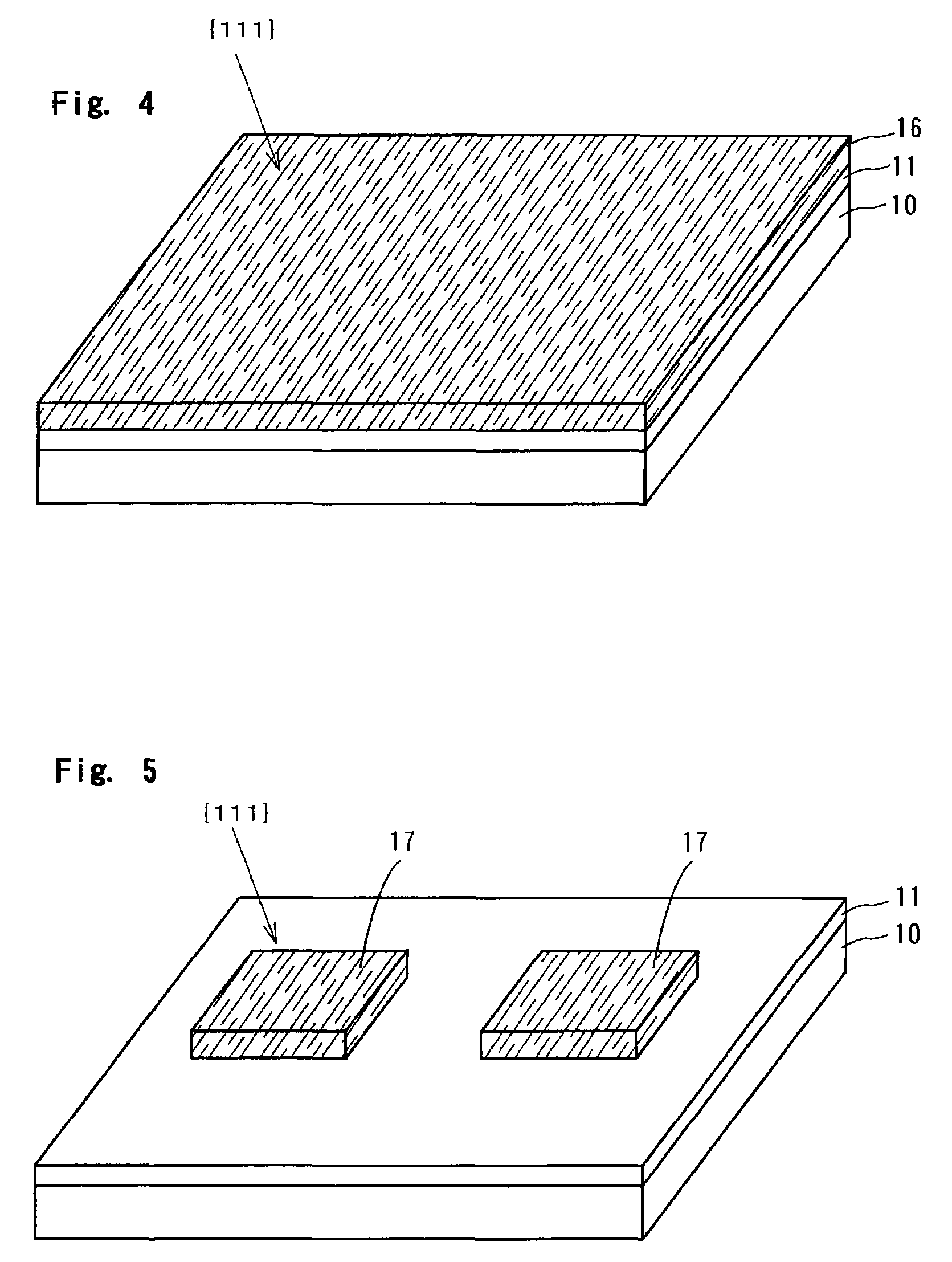
[0167]According to Embodiment 1, the crystal orientation of the first crystalline semiconductor film is predominantly oriented to {111} by selectively adding the metal element. In contrast thereto, according to the embodiment, an explanation will be given of a method of forming a first crystalline semiconductor film predominantly oriented to {101} by using a silicon film added with germanium as a first amorphous semiconductor film.

[0168]Refer to FIG. 9

[0169]First, similarly to Embodiment 1, the base film 11 is formed on the substrate 10 and a silicon film 42 added with amorphous germanium is formed on the base film 11 as a first amorphous semiconductor film. As a method of forming the silicon film 42, a publicly-known film forming method of a sputtering method, a plasma CVD method, a low pressure CVD method or the like can be adopted.

[0170]When the plasma CVD method is applied, a reaction gas comprising SiH4 and GeH4, or a reaction gas comprising GeH4 diluted by SiH4 and H2 is added...

embodiment 3

[0223]According to the example, an explanation will be given of an example of forming a lower layer of a first crystalline semiconductor layer by irradiating continuous wave laser and crystallizing an upper layer of a second amorphous semiconductor layer with the first crystalline semiconductor layer as a seed by irradiating continuous wave laser beam.

[0224]Refer to FIG. 15

[0225]First, similarly to Embodiment 1, the base film 11 is formed on the substrate 10 and an amorphous silicon film 52 is formed on the base film 11 as a first amorphous semiconductor film. As a forming method, a publicly-known film forming method of a sputtering method, a plasma CVD method or a low pressure CVD method can be adopted.

[0226]Refer to FIG. 16

[0227]Next, the first amorphous semiconductor film 52 is crystallized by irradiating continuous wave laser beam. Laser beam is irradiated while moving the irradiated region 21 produced by the continuous wave laser beam relative to the substrate 10 in a direction...


PUM


Abstract

To provide a thin film transistor having a high field effect mobility and a small variation in characteristics thereof, a second amorphous semiconductor layer patterned in a predetermined shape is formed on a first crystalline semiconductor layer 17 for constituting source and drain regions. By irradiating an irradiated region 21 of continuous wave laser beam while scanning along a channel length direction, the second amorphous semiconductor layer is crystallized to form a second crystalline semiconductor layer 22. The first crystalline semiconductor layer 17 is crystallized by selectively adding nickel and therefore, an orientation rate of {111} is increased. By irradiating laser beam, crystals of the second amorphous semiconductor layer grow by constituting a seed by the first crystalline semiconductor layer 17 oriented to {111} and therefore, a region 22a for constituting a channel forming region is also oriented highly to {111} and a direction of a crystal grain boundary becomes parallel with the channel length direction.

Description

BACKGROUND OF THE INVENTION[0001]1. Field of the Invention[0002]The present invention relates to a semiconductor device in which an active layer is formed of a crystalline semiconductor film having a crystal structure and a method of forming the same. Particularly, the invention relates to a thin film transistor in which an active region is formed of a crystalline semiconductor film, a semiconductor device such as an integrated circuit using the thin film transistor and a method of forming fabricating the semiconductor device. Further, in the specification, a semiconductor device refers to general device functioning by utilizing a semiconductor characteristic, including, for example, a semiconductor integrated circuit, an active matrix type display device, and other electronic device such as an electronic device mounted with a semiconductor integrated circuit or an active matrix type display device.[0003]2. Description of the Related Art[0004]In developing an active matrix type disp...

Claims


Application Information

Patent Timeline
IPC IPC(8): H01L21/84H01L21/336H01L21/20H01L21/77H01L27/12H01L29/04H01L29/786
CPCH01L21/2026H01L27/12H01L29/045H01L29/66742H01L27/1277H01L29/78609H01L29/78675H01L29/78684H01L29/66757H01L29/78645H01L21/02683H01L21/02502H01L21/02422H01L21/02488H01L21/02496H01L21/02609H01L21/0242H01L21/02672H01L21/0262H01L21/02686H01L21/02516H01L21/02532H01L21/02598H01L21/0245H01L21/02381H01L21/02513H01L21/02691
Inventor HAYAKAWA, MASAHIKO
Owner SEMICON ENERGY LAB CO LTD
Why Eureka
Try Eureka