Semiconductor device, semiconductor layer and production method thereof

a semiconductor and semiconductor layer technology, applied in the direction of sustainable manufacturing/processing, crystal growth process, final product manufacturing, etc., can solve the problems of difficult to obtain crystal layer having good quality, difficult to construct environmental-resistant semiconductor devices having high breakdown voltage,

Inactive Publication Date: 2008-01-01
SHOWA DENKO KK
View PDF37 Cites 8 Cited by
  • Summary
  • Abstract
  • Description
  • Claims
  • Application Information

AI Technical Summary

Benefits of technology

[0019]The present invention has been made in light of these circumstances and the object of the present invention is to clarify the construction of a BP layer having a band gap of 2.8 to 3.4 electron volts (eV) at room temperature or a boron phosphide (BP)-base mixed layer containing boron phosphide, represented by the formula of BαAlβGaγIn1−α−β−γPδAsεN1−δ−ε (0<α≦1, 0≦β<1, 0≦γ<1, 0<α+β+γ≦1, 0<δ≦1, 0≦ε<1, 0<δ+ε≦1), the construction of a semiconductor device having the above-described BP layer or BP-base mixed crystal layer, and the construction of a production method for the BP layer or BP-base mixed crystal layer, and thereby to provide a semiconductor device which has improved and enhanced semiconductor device properties, a semiconductor layer therefor, and a production method of the semiconductor layer.

Problems solved by technology

This small band gap gives rise to a problem in that an environment-resistant semiconductor device having a high breakdown voltage cannot be readily constructed from the boron phosphide (BP) crystal layer.
Therefore, in constructing a heterojunction light-emitting part of a conventional boron phosphide (BP)-based light-emitting device, there is a problem in that the clad layer cannot be composed of boron phosphide (BP) having a room temperature band gap of about 2 eV.
However, it is well known that as the number of elements constituting the mixed crystal increases, a higher level technique is required, for example, to control the composition ratio of the constituent elements and, moreover, a crystal layer having good quality is more difficult to obtain (refer to Handotai Debaisu Gairon (Outline of Semiconductor Devices), page 24).
Thus, in view of layer formation, conventional techniques have a problem in that a BP mixed crystal layer as a barrier layer cannot be readily and simply formed.
However, this is a polycrystalline layer and is not necessarily suitable for the construction of an active layer or a functional layer of a semiconductor device.
In a wide gap semiconductor having such a large band gap, the control of the conduction type by impurity doping and the control of carrier density are difficult.
However, despite the layer formation of BP crystal layers heretofore practiced using a vapor-phase growth method or the like, a method for forming a BP crystal layer which gives a band gap of about 3 eV has not yet been disclosed.

Method used


Image

  • Semiconductor device, semiconductor layer and production method thereof
  • Semiconductor device, semiconductor layer and production method thereof
  • Semiconductor device, semiconductor layer and production method thereof

Examples


example 1

[0119]In Example 1, the present invention is described in detail by referring to a Group III nitride semiconductor LED using the BP semiconductor layer of the present invention. FIG. 6 schematically shows a cross sectional structure of the pn junction type LED 60 of Example 1.

[0120]The stacked layer structure 61 for use in LED 60 was constructed using a boron (B)-doped p-type Si single crystal having a (111) plane as the substrate 601. The low-temperature buffer layer 602 on the substrate 601 was composed of boron phosphide (BP) with the main part being amorphous in the as-grown state. The low-temperature buffer layer 602 was grown at 350° C. by an atmospheric pressure MOCVD method using a triethylborane ((C2H5)3B) / phosphine (PH3) / hydrogen (H2) system. The layer thickness of the low-temperature buffer layer 602 was about 12 nm.

[0121]Using the above-described MOCVD vapor phase growth method, a magnesium-doped p-type BP layer was stacked at 950° C. as a lower clad layer 603 on the sur...

example 2

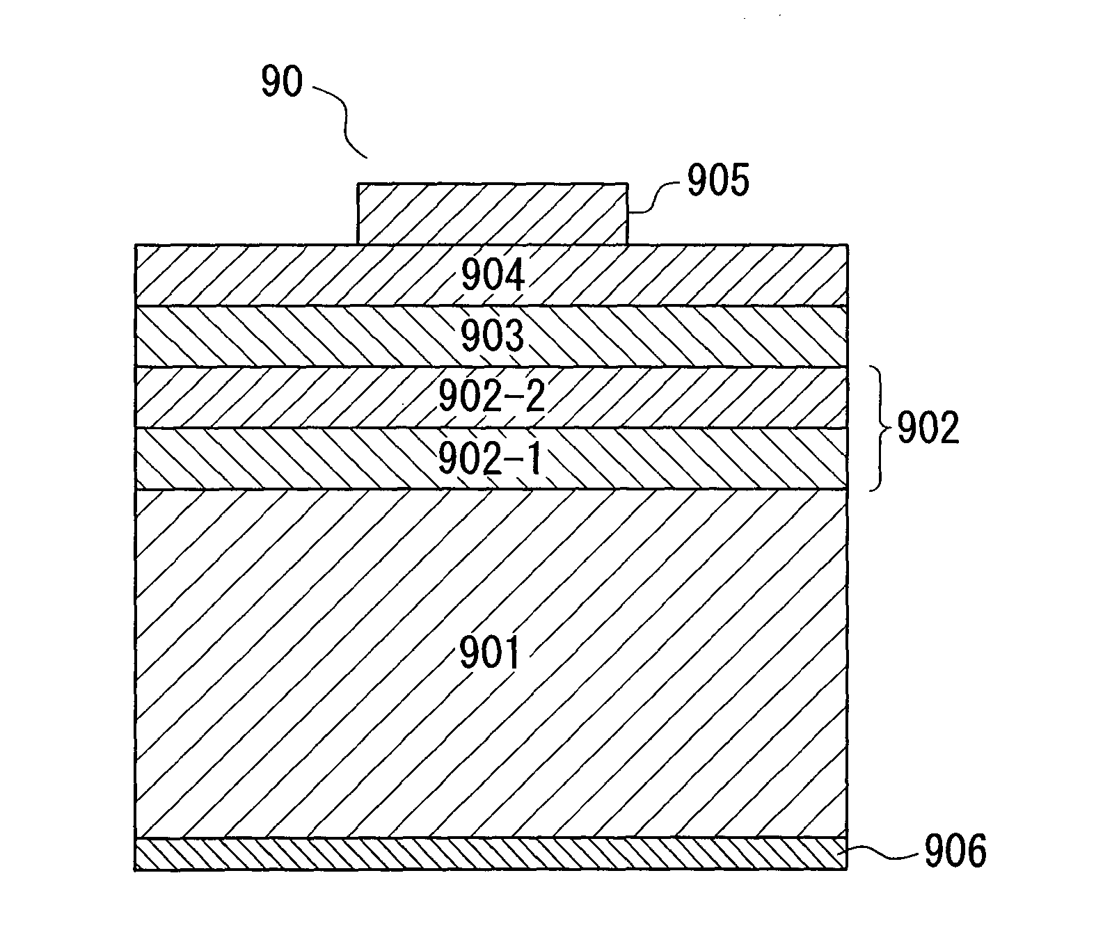
[0128]In Example 2, the present invention is described in detail by referring to a pn junction-type diode having the boron phosphide (BP) layer specified in the present invention. FIG. 9 schematically shows a cross sectional structure of the pn junction-type diode 90 of Example 2.

[0129]On a phosphorus (P)-doped n-type Si single crystal substrate 901 having a (111) plane, a low-temperature crystal layer 902-1 composed of boron gallium phosphide (BXGa1−XP) was stacked at 400° C. by a reduced pressure MOCVD method using a diborane (B2H6) / (CH3)3Ga / H2 system. The boron (B) composition ratio (═X) was set to 0.02 so as to attain lattice-matching to the Si single crystal (lattice constant=0.5431 nm). The low-temperature crystal layer 902-1 was grown under reduced pressure of about 1.3×10⁴ pascals (Pa). The layer thickness of the low-temperature crystal layer 902-1 was about 4 nm.

[0130]When observed by a sectional TEM method, in the B0.02Ga0.98P low-temperature crystal layer 902-1 in the as-...

example 3

[0137]In Example 3, the present invention is described in detail by referring to an npn junction-type hetero bipolar transistor (HBT) having the BP-base mixed crystal containing boron phosphide (BP) of the present invention. FIG. 11 is a schematic sectional view of the npn junction-type HBT 10 of Example 3.

[0138]On a phosphorus (P)-doped n-type Si single crystal substrate 101 having a (100) plane, a low-temperature buffer layer 102 composed of boron gallium phosphide (BXGa1−XP) was stacked at 350° C. by a reduced pressure MOCVD method using a diborane (B2H6) / (CH3)3Ga / H2 system. The boron (B) composition ratio (═X) was set to 0.02 so as to attain lattice-matching to the Si single crystal (lattice constant=0.5431 nm). The low-temperature buffer layer 102 was grown under a reduced pressure of about 1.3×10⁴ pascals (Pa). The layer thickness of the low-temperature buffer layer 102 was about 14 nm.

[0139]On the B0.02Ga0.98P low-temperature buffer layer 102, respective functional layers sho...


PUM

PropertyMeasurementUnit
band gapaaaaaaaaaa
band gapaaaaaaaaaa
temperatureaaaaaaaaaa

Abstract

A semiconductor device is prepared by the use of a vapor phase method and is provided with a semiconductor layer composed of boron phosphide (BP) having a band gap at room temperature of not less than 2.8 eV and not more than 3.4 eV or a boron phosphide (BP)-base mixed crystal which contains the boron phosphide (BP) and which is represented by the formula: BαAlβGaγIn1−α−β−γPδAsεN1−δ−ε (0<α≦1, 0≦β<1, 0≦γ<1, 0<α+β+γ≦1, 0<δ≦1, 0≦ε<1, 0<δ+ε≦1).

Description

[0001]This application claims benefit of U.S. provisional Application No. 60 / 300,425 filed Jun. 26, 2001, under 35 U.S.C. § 119(e).TECHNICAL FIELD[0002]The present invention relates to: a boron phosphide (BP) layer having a band gap of 2.8 to 3.4 electron volts (eV) at room temperature or a boron phosphide (BP)-base mixed crystal layer containing boron phosphide, represented by the formula βαAlβGaγIn1−α−β−γPδAsεN1−δ−ε (wherein 0<α≦1, 0≦β<1, 0≦γ<1, 0<α+β+γ≦1, 0<δ≦1, 0≦ε<1, 0<δε≦1); a semiconductor device having the BP layer or BP-base mixed crystal layer; and a production method of the BP layer or BP-base mixed crystal layer.BACKGROUND ART[0003]Group III-V compound semiconductors comprising boron (B) which belongs to Group III of the Periodic Table, and an element which belongs to Group V include boron nitride (BN), boron phosphide (BP), and boron arsenide (BAs). For example, hexagonal boron nitride (BN) is an indirect transition-type semiconductor having a band ...

Claims


Application Information

Patent Timeline
Patent Type & Authority Patents(United States)
IPC IPC(8): H01L33/00C30B25/02H01L21/18H01L21/20H01L21/205H01L21/335H01L27/15H01L29/20H01L29/201H01L29/205H01L29/778H01L31/0304H01L31/18H01L33/12H01L33/30
CPCC30B25/02C30B29/40C30B29/406H01L21/0237H01L21/02381H01L21/0242H01L21/02455H01L21/02461H01L21/02538H01L21/02543H01L21/0262H01L29/2003H01L29/201H01L29/205H01L29/66462H01L29/7783H01L31/03046H01L31/1852H01L33/30Y02E10/544Y02P70/50H01L21/20
Inventor UDAGAWA, TAKASHI
Owner SHOWA DENKO KK
Why Eureka
Try Eureka