Process for producing printed wiring board and photosensitive resin composition used in the same

a resin composition and printing technology, applied in the direction of photosensitive materials, instruments, photomechanical equipment, etc., can solve the problems of poor mechanical strength, poor yield of jointing, and high cost of gold plating

Inactive Publication Date: 2008-03-04
HITACHI CHEM CO LTD
View PDF16 Cites 9 Cited by
  • Summary
  • Abstract
  • Description
  • Claims
  • Application Information

AI Technical Summary

Benefits of technology

[0013]The present invention is directed to a photosensitive resin composition for use in printed w

Problems solved by technology

Gold plating is expensive and such soft that the Mohs hardness is 2.5.
However, we have found that the printed wiring board formed by an electroless plating method has a problem in that it has poor mechanical strength due to phosphorus contained in the Ni plating layer and has poor yield of the jointing and hence, it has low solder ball connection reliability, as compared to the wiring board formed by the conventional electrolytic plating.
In addition, we have found problems not only in that the solder ball connection reliability is low, but also in that the steps are inc

Method used


Image

  • Process for producing printed wiring board and photosensitive resin composition used in the same
  • Process for producing printed wiring board and photosensitive resin composition used in the same
  • Process for producing printed wiring board and photosensitive resin composition used in the same

Examples


example 1

[0091](a) A solution of the photosensitive resin composition of the present invention having the formulation of materials shown in Table 1 was obtained.

[0092](b) The solution of the photosensitive resin composition obtained in the previous step was coated onto a polyethylene terephthalate film (hereinafter, referred to as “PET”) having a (width: 380 mm×thickness: 20 μm) size so that the dried film had a thickness of 50 μm. The resultant film was dried at 100° C. using a hot-air convection dryer, and a polyethylene film having a thickness of 35 μm was placed on the dried film, followed by press-coating by means of rolls, to obtain a photosensitive element in the present invention.

examples 2 to 12

[0093]Photosensitive elements in the present invention were individually obtained in accordance with substantially the same procedure an in Example 1 except that the formulation of ingredients was changed to those shown in Table 1.

[0094]The formulations of the photosensitive resin compositions in Examples 1 to 12 are shown in Table 1. In the Table, the unit is part(s) by weight. The weight of the binder polymer is shown in terms of a nonvolatile content.

[0095]

TABLE 1Exam-Exam-Exam-Exam-Exam-Exam-Exam-Exam-Exam-Exam-Exam-Exam-pleplepleplepleplepleplepleplepleple123456789101112Binder polymer606060606060606060606060Bisphenol A polyoxyethylene—————20———20——dimethacrylate (BPE-500)Bisphenol A polyoxyethylene————4020302040203020dimethacrylate (BPE-1300)EO,PO-modified urethane——————10———10—dimethacrylate (UA-13)EO-modified trimethylolpropane———————10———10triacrylate (TA-401)Polypropylene glycol diacrylate——2010———10———10(APG-400)Polyethylene glycol dimethacrylate40—20—————————(4G)Polyethyl...

examples 1 to 8

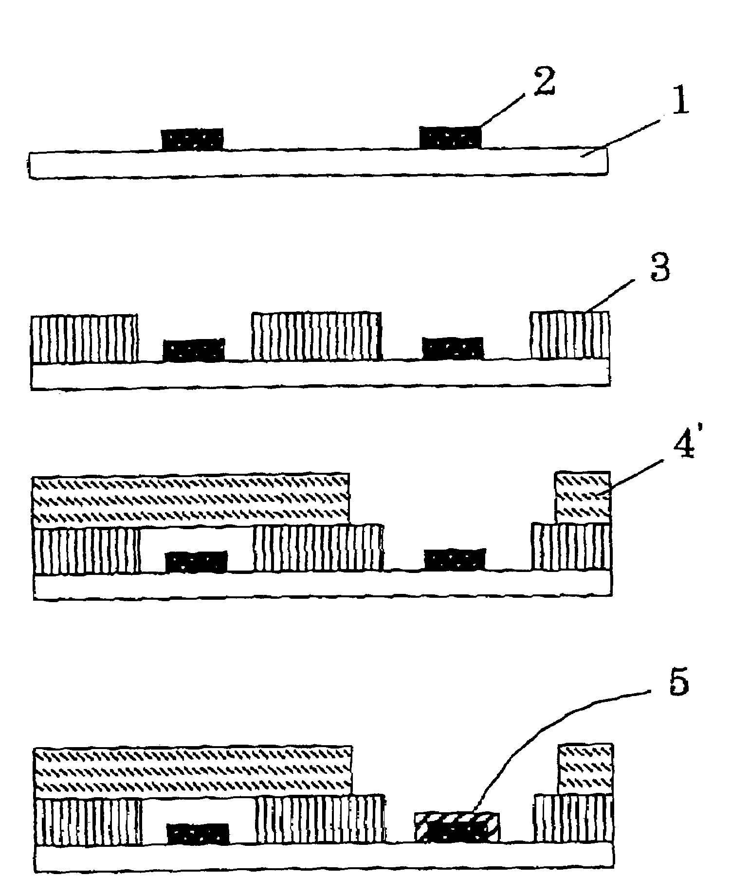
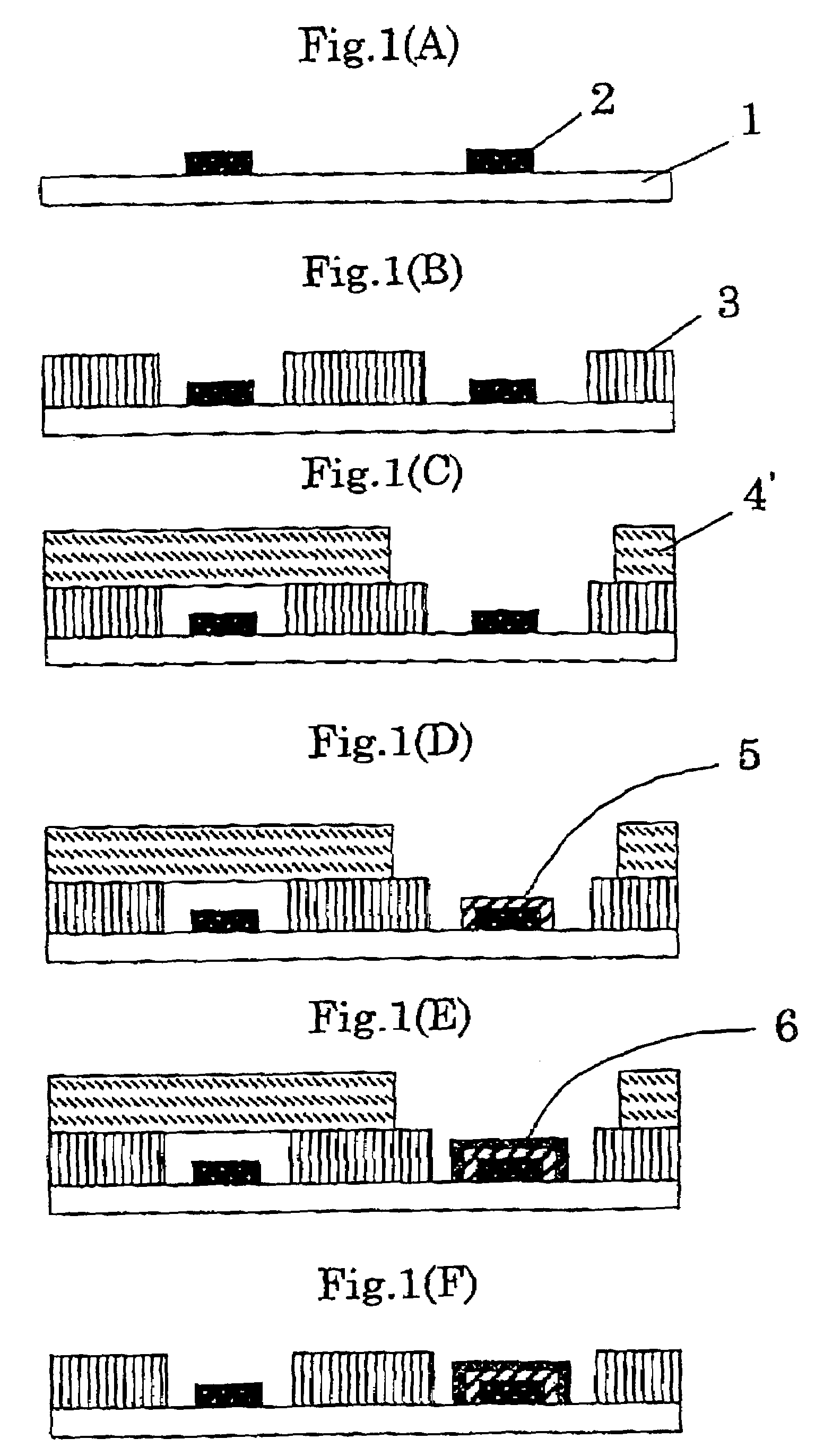
[0096]An etching resist was formed on the surface of a copper foil of a copper-clad epoxy laminate (MCL-E-67; manufactured by Hitachi Chemical Co., Ltd.) having a size of width: 12.5 cm×length: 20 cm×thickness. 1.6 mm, and an unnecessary copper foil was etched away, and metal terminals (pads) and a circuit for wiring were formed and then, the residual etching resist was stripped to obtain a wiring board having a circuit.

[0097]A photoresist (PSR-4000; manufactured by TAIYO INK MFG. CO., LTD) was coated to the entire surface of the obtained wiring board having a circuit, and then dried at 80° C. for 30 minutes. Then, excluding the pad portions, the entire surface was exposed through a mask pattern (phototool) using an exposure machine (HMW-590; manufactured by ORC Manufacturing Co., Ltd.). The unexposed portions (pad portions) were subjected to spray development using a 1% by weight aqueous solution of sodium carbonate (30° C.) to remove the photoresist on the pad portions, thus formi...


PUM


Abstract

An object of the present invention is to provide a process for producing a printed wiring board, which is advantageous not only in that the reduction in size and increase in density of the wiring board are achieved and further the steps are simplified, but also in that the connection reliability of mount parts and the yield are improved, and a photosensitive resin composition used in the process. The present invention is directed to a process for producing a printed wiring board, comprising the steps of: (i) forming a solder resist on a wiring board having a circuit; (ii) laminating a preliminarily molded layer of a photosensitive resin composition on the solder resist; (iii) subjecting the layer of the photosensitive resin composition to exposure and development to form a resist pattern of the photosensitive resin composition; (iv) subjecting the entire surface of the resultant board to electroless plating, and (v) stripping the layer of the photosensitive resin composition, wherein the steps are conducted in this order, as well as a photosensitive resin composition and the layer thereof used in the process.

Description

[0001]This is a National Phase Application in the United States of International Patent Application No. PCT / JP02 / 03147 filed Mar. 29, 2002, which claims priority on Japanese Patent Application No. 2001-096367, filed Mar. 29, 2001. The entire disclosures of the above patent applications are hereby incorporated by reference.FIELD OF THE INVENTION[0002]The present invention relates to a process for producing a printed wiring board and a photosensitive resin composition used in the same. More particularly, the present invention is concerned with a process for producing a printed wiring board, which can simplify the steps and improve the connection reliability of mount parts and the yield, and a photosensitive resin composition used in the process.BACKGROUND ART[0003]Conventionally, in the field of printed wiring board fabrication, for protecting the circuits and lowering the contact resistance and the like, the circuits are processed by metal plating. Further, as portable electronic app...

Claims


Application Information

Patent Timeline
IPC IPC(8): G03F7/20G03F7/032G03F7/26G03F7/30G03F7/42H05K3/24H05K3/28
CPCH05K3/243H05K3/28H05K2203/0571H05K2203/0574H05K2203/0588H05K2203/072G03F7/027
Inventor AKAHORI, TOSHIHIKOSAWABE, KENNATORI, MICHIKOAOKI, TOMOAKIKAJIWARA, TAKUYA
Owner HITACHI CHEM CO LTD
Why Eureka
Try Eureka