Method of growing electrical conductors

a technology of electrical conductors and growth methods, applied in the direction of electrical equipment, chemical vapor deposition coatings, coatings, etc., can solve the problems of difficult to attach source chemical molecules to the surface, drawbacks of ald-type growth of metal thin films, and difficult to deposit high-quality elemental metal thin films, etc., to achieve excellent step coverage of conductive thin films

Inactive Publication Date: 2009-02-24
ASM INTERNATIONAL
View PDF75 Cites 109 Cited by
  • Summary
  • Abstract
  • Description
  • Claims
  • Application Information

AI Technical Summary

Benefits of technology

[0045]Embodiments described herein provide methods of producing high quality conductive thin films with excellent step coverage, uniform thickness over a large area and excellent adhesion properties. The thin films may be used, for example, as seed layers for the electrodeposition of metal layers, and gate metals in thin film transistors and capacitors of advanced high-density integrated circuits.
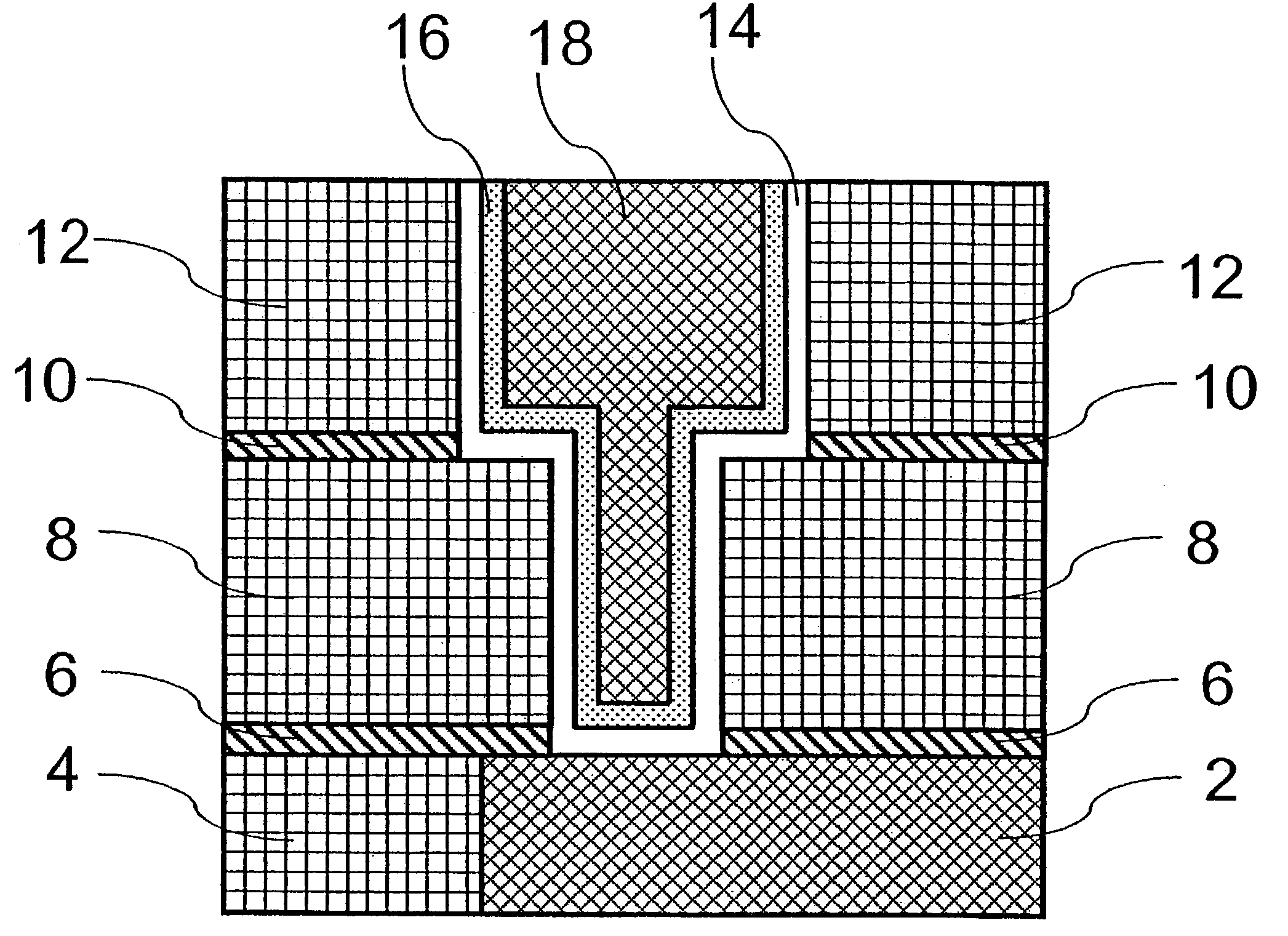
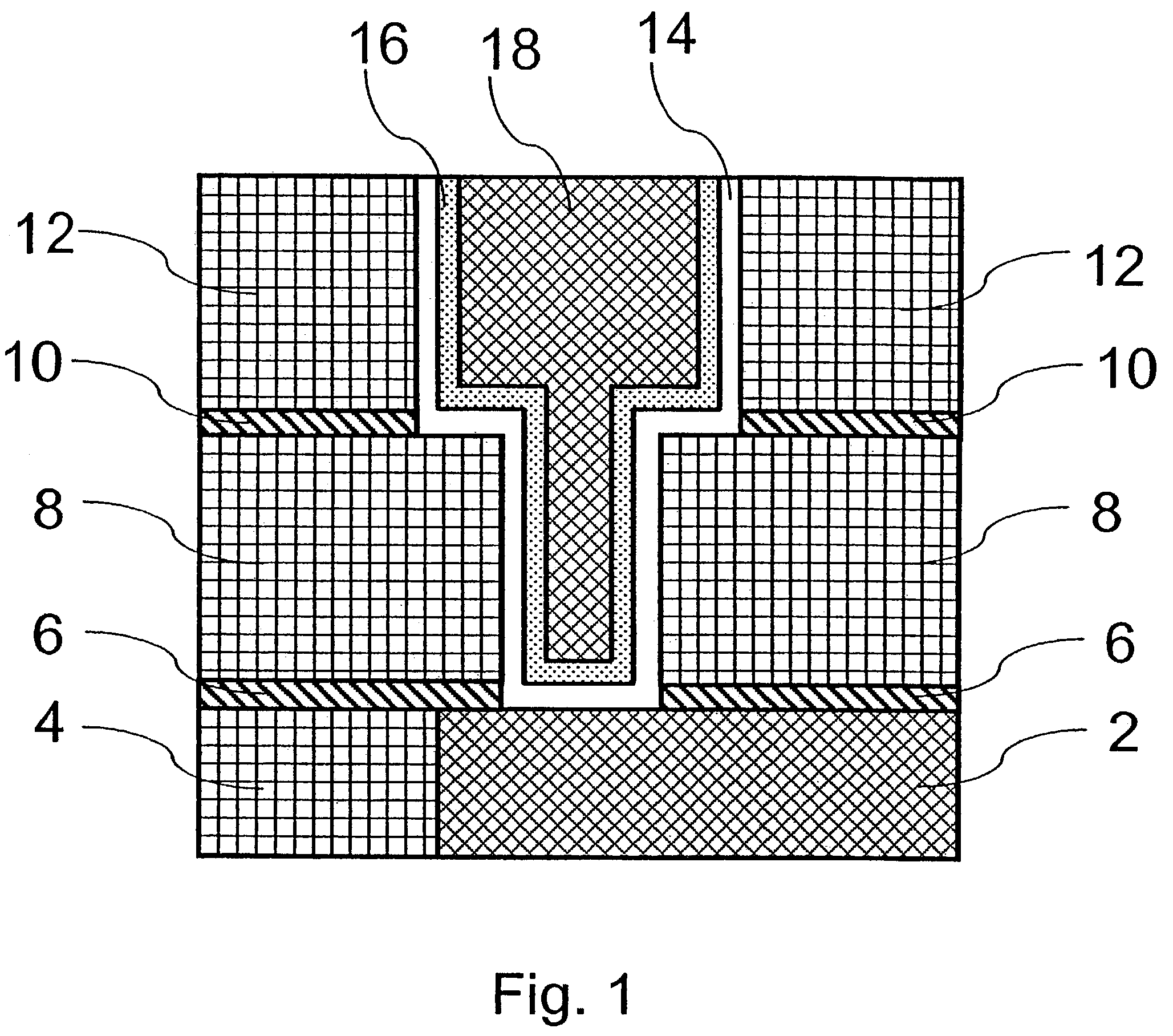
[0052]Certain embodiments described herein are especially beneficial for making electrically conductive layers in structures that have high aspect ratios, like vias, trenches, local high elevation areas and other similar surface structures that make the surface rough and thin film processing complicated by conventional CVD and PVD methods. An ALD metal oxide process combined with a reduction step provides excellent step coverage of conductive thin films on all surface formations.

Problems solved by technology

However, due to the fact that ALD is based on sequential self-saturating surface reactions of source chemical compounds, depositing high quality elemental metal thin films by ALD is very difficult.
Usually the growth rate is well below one molecular layer / cycle because the adsorbed source chemical molecules may be bulky or because substrate temperature affects the number of active sites (e.g. —OH groups) on the surface.
Experiments have revealed a drawback of the growth of metal thin films by an ALD type method.
In the case of metal deposition it is difficult to attach source chemical molecules to the surface because essentially no active sites exist on the surface.
The metal film grown is often non-uniform over an area of the substrate and it is easily peeled off from the surface, which indicates very poor adhesion of the film to the substrate.
Reproducibility of such an ALD metal growth process has traditionally been poor and the reactions do not take place at all on insulating surfaces like silicon oxide.
Thus, the deposition time for a 10-nm copper seed layer would be over 5 hours, which is uneconomical for wafer processing.
With increasing aspect ratio it is becoming difficult to get sufficient step coverage for the seed layer with the state of the art technology.
Decreasing the distance between the conductors causes voltage breakdown when the insulator thickness is too thin to hold the voltage.
However, high-k dielectrics create new problems, since they donate oxygen to the conductor and thus the capacitor properties deteriorate.
But it is difficult to deposit thin films with good step coverage on new capacitor structures with small feature size and aggressive aspect ratio.
They used Ta2O5 as an insulator while the electrodes consisted of ruthenium which was deposited by CVD from Ru(EtCp)2 and gaseous oxygen at 300-400° C. Problems related to the method included poor step coverage and reaction speed sensitivity.
The reaction of Ru(EtCp)2 with O2 was adversely affected by the partial pressures of the said compounds.
However, several problems are associated with the use of poly-Si gate electrodes.
Poly-Si is thermodynamically unstable against high dielectric constant materials at high processing temperatures.
Refractory metals have been suggested for gate metals but the stability of the metal-gate oxide interface has been an issue.
However, appropriate methods of depositing high-quality platinum group metal thin films for gate electrode applications have not yet been developed.
However, they had problems with the quality of the nickel film: pinholes were formed on the thin films during the reduction of NiO with hydrogen gas.

Method used


Image

  • Method of growing electrical conductors
  • Method of growing electrical conductors
  • Method of growing electrical conductors

Examples


example 1

ALD of Copper Oxide, Method I

[0174]The deposition was carried out in an F-200 ALCVD™ reactor manufactured by ASM Microchemistry Oy, Finland. Cu(thd)2 was loaded into an external source container and heated to 180° C. The flow of the O3 / O2 mixture was set to 120 std.cm3 / min. There was about 15% of O3 in O2. A 200 mm silicon wafer was loaded through a load lock into the reaction chamber of the reactor. The pressure of the reaction chamber was adjusted to about 5-10 mbar with a vacuum pump and flowing nitrogen gas. The reaction chamber was then heated to 210° C. One pulsing cycle consisted of 0.5 s Cu(thd)2 pulse, 1.0 s N2 purge, 0.5 s O3 pulse and 1.0 s N2 purge. The pulsing cycle was repeated 3000 times. The thin film grown on the wafer had a brownish gray color, high resistivity and excellent adhesion. The thin film consisted of CuO, which was treated with an organic reducing agent to create a metallic copper metal film on the wafer. The reduced thin film had good conductivity and s...

example 2

ALD of Copper Oxide, Method II

[0175]The deposition of copper oxide was carried out according to Example 1, with CuCl used as the copper source chemical. Pieces of silicon substrates with and without a TiN coating were loaded into the reaction chamber of the reactor. CuCl was loaded into a source tube and the reactor was evacuated. The pressure of the reaction chamber was adjusted to about 3-10 mbar with a vacuum pump and flowing N2 gas. The reaction chamber was heated to 380° C. and CuCl to about 360° C. Copper oxide grew in a controlled manner and with excellent adhesion to both of the substrates and had the same performance as the CuO film obtained in Example 1.

example 3

ALD of Copper Oxide, Method III

[0176]Surprisingly, it was found that copper oxide (Cu2O) can be grown by ALD using anhydrous copper nitrate Cu(NO3)2 and an aqueous solution of NH3 as source chemicals. It turned out that dry gaseous ammonia does not form Cu2O with anhydrous copper nitrate.

[0177]Cu(NO3)2 was synthesized according to the instructions of C. C. Addison et al. (J. Chem. Soc. (1958) pp. 3099-3106). Wet NH3 vapour was formed by evaporating aqueous solution of NH3 at room temperature from an external source bottle. The temperature of the Cu(NO3)2 source tube was set to 120° C. Silicon and TiN-coated silicon were used as substrates. The substrate temperature was about 150° C. Higher substrate temperatures were also tested. However, it was found that it is difficult to control the film uniformity at higher growth temperatures, possibly because of the thermal decomposition of copper nitrate in gas phase.

[0178]One pulsing cycle consisted of four steps, in the following order: Cu...


PUM

PropertyMeasurementUnit
thickaaaaaaaaaa
thicknessaaaaaaaaaa
thicknessaaaaaaaaaa

Abstract

A method for forming a conductive thin film includes depositing a metal oxide thin film on a substrate by an atomic layer deposition (ALD) process. The method further includes at least partially reducing the metal oxide thin film by exposing the metal oxide thin film to a reducing agent, thereby forming a seed layer. In one arrangement, the reducing agent comprises one or more organic compounds that contain at least one functional group selected from the group consisting of —OH, —CHO, and —COOH. In another arrangement, the reducing agent comprises an electric current.

Description

CLAIM OF PRIORITY[0001]The present application is a continuation-in-part of U.S. patent application Ser. No. 10 / 300,169, filed Nov. 19, 2002 now U.S. Pat. No. 6,887,795 which is a continuation of U.S. patent application Ser. No. 09 / 858,820, filed May 15, 2001, issued Nov. 19, 2002 as U.S. Pat. No. 6,482,740 B2 which claims the benefit under 35 U.S.C. §119(a) of Finnish Patent Application No. 20001163, filed May 15, 2000, each of which are incorporated in their entireties by reference herein.BACKGROUND OF THE INVENTION[0002]1. Field of the Invention[0003]The present invention relates generally to the manufacturing of integrated circuits (ICs), and particularly to the seed layers in damascene and dual damascene processes, gate metals of thin film transistors and capacitor electrodes in ICs.[0004]More particularly the present invention relates to a method of depositing seed layers for a damascene and dual damascene structures, gate metals of thin film transistors and capacitor electrod...

Claims


Application Information

Patent Timeline
Patent Type & Authority Patents(United States)
IPC IPC(8): H01L21/31H01L21/44H01L21/285H01L21/3105H01L21/768
CPCC23C16/40C23C16/406C23C16/408C23C16/45525C23C16/56H01L21/28562H01L21/3105H01L21/76843H01L21/76861H01L21/76862H01L21/76873H01L21/76874H01L21/76886
Inventor KOSTAMO, JUHANASOININEN, PEKKA J.ELERS, KAI-ERIKHAUKKA, SUVI
Owner ASM INTERNATIONAL
Why Eureka
Try Eureka