Processing apparatus with a chamber having therein a high-corrosion-resistant sprayed film

a processing apparatus and film technology, applied in chemical/physical/physico-chemical processes, transportation and packaging, coatings, etc., can solve the problems of aluminum alloys that are greater in resistance value, unsuitable, and offer the possibility of deteriorating the electrical characteristic, etc., of the device, and achieve high-corrosion-resistant properties

Inactive Publication Date: 2010-12-07
TOKYO ELECTRON LTD
View PDF282 Cites 30 Cited by
  • Summary
  • Abstract
  • Description
  • Claims
  • Application Information

AI Technical Summary

Benefits of technology

[0013]An object of the present invention is to provide a processing apparatus having a chamber applied to a film forming apparatus, heat processing apparatus and etching apparatus and having a high-corrosion-resistant property and less liable to deposit a product by a process gas or a product, such as an etching product, on its inner wall thereof.

Problems solved by technology

If the aluminum connection line and underlying silicon (Si) substrate are directly contacted with each other, there is a risk that there will occur a “Si-sucking-up” effect of aluminum, etc., at its boundary area and an alloy will be newly formed there.
The alloy thus formed is greater in the value of a resistance and is not desirable from the standpoint of a power saving and high-speed operation demanded of a resultant device.
Further, when tungsten or tungsten alloy is used as a burying layer in the contact hole, WF6 gas intrudes into the silicon substrate, thus offering a possibility of deteriorating the electrical characteristic, etc., of the device.
However, such a higher dielectric constant material is not stabler in characteristic than SiO2 conventionally used as the capacitor gate material.
If a poly-Si is used on the overlying electrode, it is oxidized due to the chemical reaction after the formation of the capacitance, thus failing to manufacture a device element of stable characteristics.
In addition, the design rules are particularly stringent.
Hence, in PVD that can hardly achieve high coverage.
In the case where the TiN film is formed by such a thermal CVD, chlorine is liable to be retained in a formed film, thus presenting a problem.
The retaining of such chlorine results in a higher specific resistance and it is not possible to obtain a proper characteristic if the film is applied to an electrode overlying a capacitor.
The lower barrier characteristic presents a problem in the case where the TiN film is used as a barrier layer for a Cu connection line or an oxygen diffusion barrier for Ta2O5 connection line of an electrode overlying the capacitor.
That is, a problem occurs due to the corrosion of the Cu connection line by the residual chlorine or a lowering of a capacitance of Ta2O5 by the diffusion of oxygen.
However, a high temperature process is not preferable due to a problem, such as thermal resistance and the corrosion, of a connection line material such as Cu and Al.
Although a chamber made of quartz or alumina is used in the formation of the TiN film by the ICP-CVD, it is not good in a plasma-resistant characteristic and a corrosion resistance to an etching gas such as ClF3 used for cleaning the interior of the apparatus after the formation of the TiN film is not better, thus presenting a problem.
Further, in this type of CVD film formation apparatus, a deposit is formed on the inner wall of the chamber due to the introduction of a process gas from above the chamber and a foreign deposit is liable to be formed.
In the case of forming the TiN film, the plasma created is attenuated due to the deposit of a conductive film on the inner wall of the upper chamber, thus making it difficult to form a film.

Method used


Image

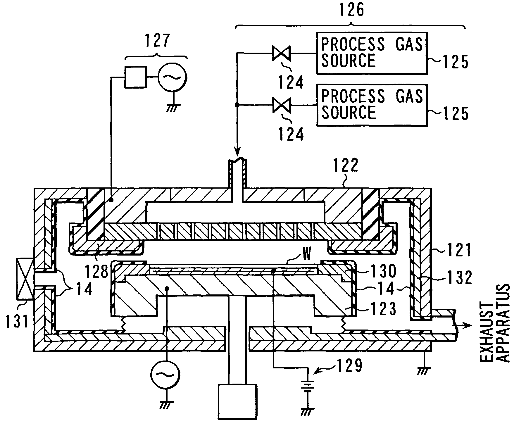
  • Processing apparatus with a chamber having therein a high-corrosion-resistant sprayed film
  • Processing apparatus with a chamber having therein a high-corrosion-resistant sprayed film
  • Processing apparatus with a chamber having therein a high-corrosion-resistant sprayed film

Examples


first embodiment

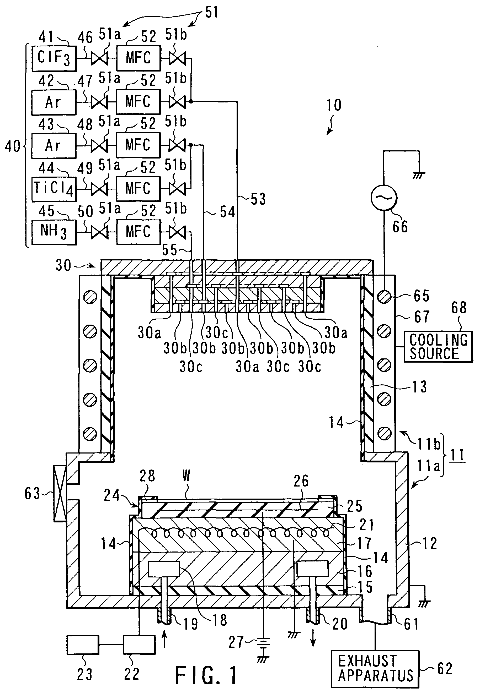
[0042]FIG. 1 is a cross-sectional view showing a practical example applied to a CVD film forming apparatus as the present invention in a processing apparatus having a mounted chamber having a high corrosion-resistant thermal sprayed film.

[0043]The film forming apparatus of the present invention is directed to forming, for example, a TiN thin film. The film forming apparatus 10 includes a chamber 11 having a lower chamber 11a and upper chamber 11b formed as an integral unit in a hermetically sealable way. The upper chamber 11b is made smaller in diameter than the lower chamber 11a. The lower chamber 11a is comprised of an electric conductor 12, such as aluminum, whose surface is anadigation processed for example. The upper chamber 11b comprises a base material 13 of, for example, a ceramic material and a sprayed film 14. The film 14 may contain oxide of Y, Sc, La, Ce, Eu, Dy2O3 or the like, or fluoride of one of these metals. The film 14 may be made of a compound of a III-b element o...

second embodiment

[0068]the present invention will be explained below.

[0069]FIG. 10 is a cross-sectional view showing a CVD apparatus according to the second embodiment. In this embodiment, a chamber, shower head and gas supply system are different in structure from those of the first embodiment. In this Figure, the same reference numerals are employed to designate parts or elements corresponding in structure to those shown in FIG. 1 and any further explanation is, therefore, omitted.

[0070]In this apparatus, an upper chamber 11c is provided above a lower chamber 11a and it is made of a ceramic material, such as Al2O3, SiO2 and AlN. At a shower head member 70 of pipe type provided at the top of the upper chamber 11c, gas discharge holes 70a, 70b and 70c are alternately formed to discharge gases toward a lower zone within the chamber. A gas supply system 40a comprises gas supply sources and valves 51 and mass flow controllers 52 as in the case of the gas supply system 40 as set out above. This embodime...

third embodiment

[0080]the present invention will be described below.

[0081]FIG. 11 is a cross-sectional view showing a CVD apparatus according to a third embodiment of the present invention.

[0082]This embodiment constitutes a combined structure of a lower chamber 11a similar to that in the first embodiment shown in FIG. 1 and an upper chamber 11c similar to that of the second embodiment shown in FIG. 10. A sprayed film 14 of mainly Al2O3 and Y2O3 having an insulating property and high corrosion resistance as set out above is formed on the inner wall of the upper chamber 11b. In this embodiment, the same reference numerals are employed to designate parts or elements corresponding in structure to those shown in FIGS. 1 and 10 and any further explanation is, therefore, omitted.

[0083]In the third embodiment, a high-corrosion-resistant sprayed film 14 is formed on the inner wall of the upper chamber 11c and, even if plasma and cleaning gas are contacted with the inner wall, is hard to be etched to provid...


PUM

PropertyMeasurementUnit
thicknessaaaaaaaaaa
weight ratioaaaaaaaaaa

Abstract

A processing apparatus of the present invention has a mounted chamber holding a semiconductor wafer and having members for work-processing the substrate under any of heating, plasma and process gas or a combination of them, in which a film of Al2O3 and Y2O3 is formed on an inner wall surface of the chamber and on those exposed surface of the members within the chamber and has a high-corrosion resistance and insulating property and, when the process gas is introduced onto a processing surface of a semiconductor wafer and diffused into it, any product is less liable to be deposited on a plasma generation area and on those members held within the chamber.

Description

CROSS-REFERENCE TO RELATED APPLICATIONS[0001]This application is based upon and claims the benefit of priority from the prior Japanese Patent Application No. 11-352018, filed Dec. 10, 1999, the entire contents of which are incorporated herein by reference.BACKGROUND OF THE INVENTION[0002]A present invention relates to a processing chamber having a mounted chamber having a high-corrosion-resistant film and applied to a film forming apparatus, heat processing apparatus and etching apparatus as used in a CVD (Chemical Vapor Deposition), etc.[0003]In response to a recent demand for a high density and high integration unit, a semiconductor device is progressed from a two-dimensional connection structure toward a three-dimensional multi-connection structure. For this reason, the burying technique for electrical interlayer connection using a contact hole for connection between an underlying circuit element and an overlying connection layer and a via hole for connection between an underlyin...

Claims


Application Information

Patent Timeline
Patent Type & Authority Patents(United States)
IPC IPC(8): C23F1/00H05B31/26H01J7/24H01L21/306C23C16/00B01J19/00B01J19/08C23C4/10C23C16/44C23C16/455C23C16/507C23C16/509C23F4/00H01J37/32H01L21/205H01L21/302H01L21/3065H01L21/31
CPCC23C4/105C23C16/4404C23C16/45514C23C16/45561C23C16/45565C23C16/4558C23C16/507H01J37/321H01J37/32477H01J37/32495C23C16/45574Y10T428/26C23C4/11
Inventor OTSUKI, HAYASHI
Owner TOKYO ELECTRON LTD
Why Eureka
Try Eureka